Automated Optical Inspection (AOI) in PCB Manufacturing: Importance, Functions, and Best Practices
Introduction
Automated Optical Inspection (AOI) is a critical machine used in PCB (Printed Circuit Board) manufacturing to detect defects, inconsistencies, and misalignments in circuit patterns, solder joints, and component placements. AOI ensures high production quality, reduces manual inspection errors, and enhances yield rates in modern PCB fabrication.
With the increasing demand for high-density interconnect (HDI) PCBs, fine-pitch components, and complex multilayer boards, AOI plays an essential role in ensuring precision, reliability, and cost-effective quality control.
This article explores the importance of AOI in PCB manufacturing, how it works, key features, advantages, limitations, and best practices for maximizing inspection efficiency and accuracy.
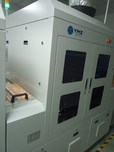
Automated Optical Inspection
What is Automated Optical Inspection (AOI)?
AOI is a machine-based visual inspection system that uses high-resolution cameras and image processing algorithms to detect PCB defects. It is widely used in pre-lamination, post-lamination, solder paste, and post-soldering stages to ensure manufacturing accuracy.
Functions of AOI in PCB Manufacturing
- Detects circuit pattern defects – Identifies shorts, opens, missing traces, and misaligned patterns.
- Ensures component placement accuracy – Verifies that resistors, capacitors, and ICs are correctly positioned and oriented.
- Inspects solder joints and connections – Detects insufficient solder, cold joints, and bridging issues.
- Reduces human inspection errors – Provides automated, repeatable, and consistent quality control.
- Improves production efficiency – Quickly identifies defects, allowing for real-time corrections in the production process.
How AOI Works: Inspection Process
The AOI process involves multiple imaging and processing steps to identify potential defects and ensure PCB compliance with design specifications.
1. Image Capture and Processing
- High-resolution cameras or laser scanners capture images of the PCB surface.
- The system uses different light sources (LED, UV, or infrared) to enhance visibility of circuit patterns and solder joints.
- Multiple angles are used to detect height variations, misalignment, or hidden defects.
2. Image Comparison with Reference Data
- The captured PCB images are compared against a golden board (reference PCB) or design files (Gerber, CAD).
- Any deviations or anomalies are flagged for review.
3. Defect Classification and Analysis
- AOI classifies defects into categories such as:
- Short circuits (unintended connections)
- Open circuits (broken traces or missing connections)
- Solder issues (bridging, insufficient solder, cold joints)
- Component misalignment (incorrect placement, polarity errors)
- The system highlights suspected defects for manual verification or automated repair.
4. Data Logging and Reporting
- AOI systems generate detailed reports and statistical data.
- Enables process optimization by identifying recurring defects.
- Improves traceability and quality control in mass production.
Types of AOI Machines
1. 2D AOI (Two-Dimensional Inspection)
- Uses top-down cameras to inspect PCB surfaces.
- Effective for detecting surface-level defects like missing traces and component misplacement.
- Less effective for inspecting solder joint quality and height variations.
2. 3D AOI (Three-Dimensional Inspection)
- Uses multiple cameras and laser profiling to detect height, volume, and shape of components and solder joints.
- Provides more accurate defect detection for solder paste inspection (SPI) and complex PCB assemblies.
- Higher cost but essential for HDI and fine-pitch PCB manufacturing.
3. Inline AOI vs. Offline AOI
- Inline AOI: Integrated into the production line for real-time defect detection and process optimization.
- Offline AOI: Used for batch inspection or detailed analysis of sampled PCBs.
Advantages of AOI in PCB Manufacturing
✅ 1. Faster and More Accurate Inspection
- Detects defects in seconds compared to manual inspection.
- Reduces operator fatigue and inconsistency.
✅ 2. Reduces Production Costs
- Early detection of defects prevents waste and rework.
- Identifies process variations, reducing long-term quality issues.
✅ 3. Increases Yield and Reliability
- Ensures higher first-pass yield rates by detecting errors before final assembly.
- Reduces defective PCBs reaching functional testing or customers.
✅ 4. Enhances Traceability and Quality Control
- Stores inspection data for quality audits and defect trend analysis.
- Helps optimize PCB manufacturing processes over time.
✅ 5. Supports High-Volume Production
- Can inspect thousands of PCBs per hour, making it ideal for mass production.
- Ensures consistent high-quality output for large-scale electronics manufacturing.
Limitations of AOI
❌ 1. Cannot Detect Internal Layer Defects
- AOI is limited to surface inspection and cannot check inner PCB layers.
- X-ray Inspection (AXI) is needed for BGA and multi-layer via defects.
❌ 2. False Positives and False Negatives
- Some AOI systems may flag non-defective areas as errors (false positives).
- Some fine defects may go undetected if machine parameters are not optimized.
❌ 3. High Initial Investment
- Advanced 3D AOI systems have a higher cost compared to manual inspection.
- However, cost savings from defect prevention and rework reduction justify the investment.
Best Practices for Using AOI in PCB Production
- Select the Right AOI Type
- Use 2D AOI for standard PCBs with moderate complexity.
- Use 3D AOI for HDI, fine-pitch, and solder paste inspection.
- Optimize Inspection Parameters
- Adjust light intensity, camera angles, and defect thresholds for accuracy.
- Reduce false alarms by fine-tuning sensitivity settings.
- Integrate AOI with Process Control Systems
- Connect AOI to MES (Manufacturing Execution Systems) to track defect trends.
- Use real-time defect analysis to improve PCB quality.
- Perform Regular Calibration and Maintenance
- Keep cameras, lenses, and lighting systems clean for clear image capture.
- Update software and algorithms to adapt to new PCB designs.
- Use AOI Data for Process Improvement
- Analyze AOI reports to identify recurring defects and improve manufacturing quality.
- Collaborate with production teams to reduce process variations.
Conclusion
Automated Optical Inspection (AOI) is a key technology in modern PCB manufacturing, ensuring defect-free circuit boards, reducing production costs, and enhancing process efficiency. By using advanced 2D and 3D AOI systems, manufacturers can achieve higher precision, faster defect detection, and improved product reliability.
While AOI has limitations, its ability to provide high-speed, accurate, and consistent quality control makes it an indispensable tool for high-density, high-reliability PCB production. Implementing AOI best practices and integrating it with process control systems will further enhance PCB quality and manufacturing efficiency for the electronics industry.

- long board pcb
- Flexible PCBs
- Special PCB
- Express Printed Circuit Board
- Pcb Prototype
- LED PCB
- PCB
- Printed Circuit Board
- Pcb meaning
- Pcb manufacturer
- Rigid pcb board
- Rigid Flex PCB
 Quote
Quote
 E-mail