In-Depth Analysis of PCB Surface Finishes: Strategic Choice Between Electroplated Gold and ENIG
- Instruction
- Electroplated Gold: The Preferred Choice for Durability
- ENIG: The Choice for Precision
- Comprehensive Comparison: Performance and Application Scenarios
- SQPCB’s Precision Manufacturing Advantages
- V. Frequently Asked Questions
- Make an Informed Choice
Instruction
In high-end PCB manufacturing, the selection of gold surface finishes directly impacts product performance, reliability, and cost. Electroplated gold and ENIG (Electroless Nickel Immersion Gold) are two mainstream processes, and understanding their differences is crucial for optimal decision-making.
I. Electroplated Gold: The Preferred Choice for Durability
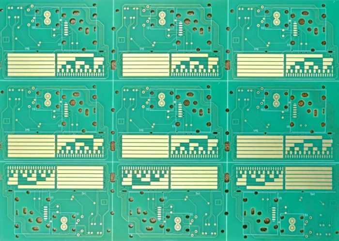
Electroplated Gold deposits a metal layer on the PCB surface through an electrochemical process. This process first applies a nickel barrier layer on the copper surface, followed by hard gold electroplating on the nickel layer.

Electroplated Gold
II. ENIG: The Choice for Precision
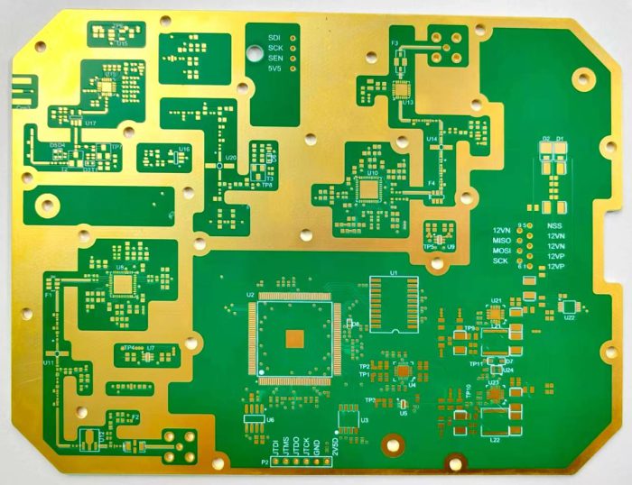
ENIG deposits a nickel-gold layer on the copper surface through a chemical replacement reaction. This process first chemically deposits a nickel-phosphorus alloy on the copper surface, followed by a thin gold layer through replacement reaction.
Why Both Processes Require a Nickel Layer?
The nickel layer plays a vital role in both processes:
Diffusion Barrier: Prevents mutual diffusion between copper and gold, avoiding the formation of brittle intermetallic compounds
Surface Planarization: Fills microscopic defects on the copper surface, providing an ideal base for gold deposition
Enhanced Durability: Provides a solid support base in electroplated gold and forms a reliable soldering interface in ENIG

Electroplated Gold
III. Comprehensive Comparison: Performance and Application Scenarios
| Characteristic | Electroplated Gold | ENIG |
|---|---|---|
| Gold Thickness | Thicker (1-3μm) | Thinner (0.05-0.1μm) |
| Nickel Layer Function | Provides hard support, enhances wear resistance | Forms phosphorus-nickel alloy, provides soldering interface |
| Wear Resistance | Excellent, suitable for frequent plugging | Average, suitable for one-time soldering |
| Surface Flatness | Poor | Excellent |
| Solderability | Average | Excellent |
| Cost | Higher | Moderate |
| Typical Applications | Gold fingers, connectors, switches | BGA, fine-pitch components, RF circuits |
IV. SQPCB’s Precision Manufacturing Advantages
At SQPCB, we deeply understand the requirements of different gold processes for precision manufacturing and have mastered large-scale production technologies for both processes. In the circuit board manufacturing field, SQPCB creates unique value for customers through the following advantages:
We have invested in industry-leading PCB manufacturing equipment to ensure exceptional quality:
Precision Imaging System:
Circuit LDI Automated Exposure Equipment: Eliminates traditional film expansion/contraction issues, improves alignment accuracy to ±15μm
Solder Mask LDI Automated Exposure Equipment: Ensures solder mask opening accuracy, perfectly matching high-density pads
Automated Text Printing Equipment: Achieves permanent, clear markings, completely avoiding manual errors
Complete Process Quality Control:
Through our own lamination production lines and surface treatment workshops (including HASL and ENIG), we achieve end-to-end control from substrate to finished product. This not only significantly reduces traditional issues such as scratches and contamination but also elevates the gloss and consistency of solder mask ink to new levels, ensuring completely controllable quality and delivery times.
V. Frequently Asked Questions
Q1: What is the specific cost difference between electroplated gold and ENIG?
A1: Electroplated gold typically costs 30-50% more than ENIG, with specific differences depending on gold thickness and processing area. Electroplated gold is more suitable for applications requiring high wear resistance, while ENIG provides a better balance between cost and performance.
Q2: Which process is more suitable for gold finger designs?
A2: Electroplated gold is the preferred choice for gold fingers. Its thicker hard gold layer can withstand repeated plugging wear, while ENIG’s thin gold layer is prone to damage under frequent friction.
Q3: Does ENIG have black pad risk? How is it prevented?
A3: Yes, the nickel layer in ENIG may experience black pad issues. We precisely control chemical solution parameters and process time, maintaining phosphorus content stable at 7-9%, and employ secondary activation processes to ensure nickel layer quality, effectively eliminating black pad phenomenon.
Q4: Which process do you recommend for BGA packaging?
A4: ENIG is the ideal choice for BGA packaging. Its excellent surface flatness ensures solder ball coplanarity, while the thin gold layer effectively prevents solder joint embrittlement, improving soldering reliability.
Q5: How does SQPCB ensure thickness uniformity in electroplated gold?
A5: We use advanced oscillating plating lines and intelligent anode design, combined with real-time monitoring systems, to ensure gold layer thickness variation does not exceed ±0.2μm across different positions. This level of precision is crucial in applications such as connector manufacturing.
Make an Informed Choice
At SQPCB, we are not only executors of processes but also your technical consultants. Whether you need the ultimate durability of electroplated gold or the precision soldering performance of ENIG, we can provide the most suitable solution. Let our professional experience safeguard your product reliability.
Contact our technical team today for personalized process recommendations tailored to your project.
- long board pcb
- Flexible PCBs
- Special PCB
- Express Printed Circuit Board
- Pcb Prototype
- LED PCB
- PCB
- Printed Circuit Board
- Pcb meaning
- Pcb manufacturer
- Rigid pcb board
- Rigid Flex PCB

 Quote
Quote
 E-mail