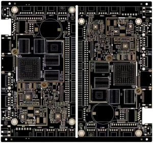
PCB refers to a bare printed circuit board with no components installed in the world of electronics,
PCBA refers to a printed circuit board assembly where all the necessary components have been mounted and soldered in place in the world of electronics.
Although the terms sound similar, they represent different stages in the electronic manufacturing process. Understanding the difference between PCB and PCBA is essential for anyone involved in electronics design, production, or repair.
PCB: The Foundation
A PCB, or Printed Circuit Board, is the foundational component of most electronic devices. It is a flat, rigid circuit board made of non-conductive material with layers of copper circuitry laminated onto it. The main functions of a PCB are to physically support and electrically connect electronic components.
difference between pcb and pcba
Components of a PCB:
Substrate: The base material of the PCB, typically made from fiberglass (FR4) or composite epoxy. It provides mechanical support and ensures the board’s durability and stability. Variants include flexible substrates for flexible PCBs and aluminum-based substrates for high-heat applications like LED lighting.
Copper Layer: A conductive layer formed by etching copper sheets, creating pathways for electrical signals. PCBs may have single-layer, double-layer, or multi-layer copper layers, depending on their complexity. Thicker copper layers are used in high-current or high-power applications.
Solder Mask: A protective coating applied over the copper traces to insulate and prevent accidental short circuits or oxidation. It also ensures a clean, polished appearance and provides a base for applying solder. Common colors include green, red, black, and blue.
Silkscreen: The top layer where component labels, symbols, and instructions are printed. This layer aids in identifying components, understanding circuit functions, and simplifying assembly and debugging processes.
Drilled Holes/Vias:Holes drilled into the board to enable connections between layers (vias) or for mounting through-hole components. Vias can be through-hole, blind, or buried, depending on the board’s design.
Surface Finish:A coating applied to the exposed copper areas to protect them and ensure solderability. Common finishes include HASL (Hot Air Solder Leveling), ENIG (Electroless Nickel Immersion Gold), and OSP (Organic Solderability Preservative).
Pads:Exposed copper areas designed for soldering electronic components. Pads can be either for through-hole or surface-mount components, tailored to the assembly process.
Dielectric Layer:An insulating layer between copper layers in multi-layer PCBs. This material ensures electrical isolation and affects signal integrity and thermal performance.
Edge Connectors/Fingers:Gold-plated contacts along the PCB edge used for connecting the board to external systems or modules, often found in PCBs used for memory modules or expansion cards.
Power and Ground Planes:Internal layers or zones dedicated to power distribution and grounding to ensure signal integrity, reduce noise, and provide stable operation for high-speed circuits.
Types of PCBs:
Single-Sided PCBs: Have one layer of copper.
Double-Sided PCBs: Have copper layers on both sides.
Multi-Layer PCBs: Consist of multiple layers of copper and insulating material.
SQPCB stands out with advanced in-house equipment, including LDI inline exposure machines for circuitry and solder mask, and inline automated legend inkjet printers. Although these investments are substantial, they ensure excellent yield rates and overcome issues common with older film-based equipment—such as dimensional expansion/shrinkage, misalignment, operator error, surface scratches, and foreign particle contamination. The result is reduced rework, improved solder mask gloss, and superior consistency. Additionally, SQPCB operates its own lamination process, as well as in-house HASL and ENIG surface finishing lines, allowing full control over quality and delivery schedules.
PCBA: The Complete Assembly
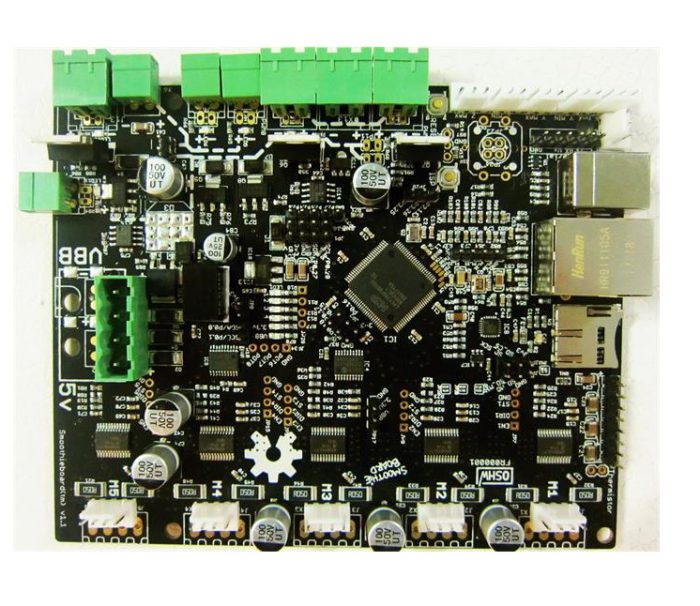
PCBA stands for Printed Circuit Board Assembly. It is the stage where all the electronic components are mounted onto the PCB. The process of creating a PCBA involves several steps, including placing and soldering components onto the board, which transforms a bare PCB into a functional electronic circuit.
PCBA Manufacturing
Steps in PCBA: A Detailed Look
The PCBA (Printed Circuit Board Assembly) process transforms a bare PCB into a fully functional electronic circuit. This multi-step process requires precision, advanced techniques, and rigorous quality control to ensure reliable performance. Below is a detailed breakdown of the key steps:
1. Component Placement
Automated Placement Machines: High-speed machines are used to place components with incredible accuracy based on the PCB design layout. These machines ensure consistency, even for complex and high-density designs.
Surface Mount Technology (SMT): Tiny components like resistors, capacitors, and ICs are mounted directly onto the surface of the PCB. SMT is ideal for compact and lightweight devices.
Manual Placement for Unique Components: While most components are placed automatically, some unique or delicate components may require manual placement to ensure precision.
2. Soldering
Reflow Soldering: Commonly used for SMT components, this technique involves applying solder paste to the PCB, placing the components, and then heating the assembly in a reflow oven. The heat melts the solder, creating strong connections.
Wave Soldering: Suitable for Through-Hole Technology (THT) components, this process involves passing the PCB over a wave of molten solder. The solder adheres to exposed metal areas, creating robust bonds.
Selective Soldering: Used for mixed-technology boards with both SMT and THT components, selective soldering precisely applies solder only where needed.
3. Inspection and Testing
Automated Optical Inspection (AOI): High-resolution cameras scan the PCBA for defects such as misplaced components, solder bridges, or missing parts.
X-Ray Inspection: Used to inspect hidden solder joints, particularly in Ball Grid Array (BGA) components, ensuring all connections are secure.
Functional Testing: Simulates the board\u2019s operating environment to verify performance and ensure that all components are functioning correctly. This step includes electrical tests and load simulations.
Components on a PCBA: A Closer Look
A PCBA is a combination of various electronic components mounted onto a PCB, turning it into a functional circuit. Below are the major components found on a typical PCBA:
1. Passive Components
Resistors: Control current flow by providing resistance, essential for circuit stability.
Capacitors: Store and release electrical energy, often used for filtering and voltage regulation.
Inductors: Used in filtering and signal processing, especially in high-frequency circuits.
2. Integrated Circuits (ICs)
These are complex semiconductor devices that perform specific functions, such as amplifiers, processors, or memory units. ICs are the brain of modern electronic devices.
3. Connectors
Connectors enable the PCBA to interface with other circuits, devices, or external systems. They ensure seamless data and power transfer.
4. Active Components
Diodes: Allow current to flow in one direction and protect circuits from voltage spikes.
Transistors: Act as switches or amplifiers, controlling the flow of current in a circuit.
Key Differences: PCB vs. PCBA
To understand the distinction between PCB and PCBA, it’s essential to consider their functionality, production stage, and complexity. Here’s a more detailed explanation:
1. Functionality
PCB: A bare board without electronic components. It serves as the structural foundation for creating electronic circuits by providing a platform for component placement and copper pathways for connectivity.
PCBA: A fully assembled and functional board with all necessary electronic components mounted, ready to be integrated into electronic devices.
2. Production Stage
PCB: Represents an intermediate stage in the PCB manufacturing process. It\u2019s primarily focused on layout design, copper pathway etching, and protective layer application.
PCBA: The final stage, where components are precisely mounted, soldered, and tested, transforming the PCB into a complete electronic circuit.
3. Complexity
PCB: The process involves designing the layout, ensuring optimal placement of copper traces, and applying layers like the solder mask and silkscreen. Although challenging, it primarily focuses on the board\u2019s physical structure.
PCBA: This stage adds complexity by introducing high-precision component placement, multiple soldering techniques, and rigorous inspection and testing. It demands both technical expertise and advanced manufacturing equipment to ensure functionality.
By understanding these distinctions, one can appreciate the integral roles that both PCB and PCBA play in the electronics manufacturing process.
Conclusion
In summary, while PCB refers to the physical board that forms the basis of electronic circuits, PCBA refers to the board after it has been fully assembled with all necessary electronic components. Understanding the distinction between these two terms is crucial for anyone working in the electronics industry, as it highlights the different stages and processes involved in creating functional electronic devices.
FAQs
1. What is the main difference between PCB and PCBA?
A PCB is a bare circuit board with no components, while a PCBA has all required components assembled and soldered.
2. Can one manufacturer provide both PCB and PCBA services?
Yes, many manufacturers, like SQPCB, offer end-to-end solutions from bare board fabrication to full assembly.
3. Why does SQPCB use LDI exposure instead of film-based methods?
LDI eliminates film-related issues such as dimensional changes, misalignment, and defects caused by manual handling.
4. How does SQPCB ensure delivery time control?
With in-house lamination, HASL, and ENIG processes, SQPCB can control both production schedules and quality without relying on external vendors.
5. Does advanced equipment improve solder mask quality?
Yes. LDI solder mask exposure enhances gloss, improves definition, and reduces defects caused by dust and scratches.

- long board pcb
- Flexible PCBs
- Special PCB
- Express Printed Circuit Board
- Pcb Prototype
- LED PCB
- PCB
- Printed Circuit Board
- Pcb meaning
- Pcb manufacturer
- Rigid pcb board
- Rigid Flex PCB
 Quote
Quote
 E-mail