Design of PCB Boards: PCB Board stands for Printed Circuit Board Board, which is a common redundancy. More accurately, it’s simply referred to as a PCB (Printed Circuit Board).
What is a PCB?
A PCB is a flat board made of insulating material (such as fiberglass or composite epoxy) with conductive pathways etched or printed onto it. These pathways, or “traces,” connect various electronic components, enabling them to work together in an electronic circuit.
Key Features of Design of PCB Boards:
- Layers:
- Single-layer: A circuit on one side of the board.
- Double-layer: Circuits on both sides of the board.
- Multilayer: Multiple layers of circuits sandwiched together for more complex applications.
- Materials: The base is typically made of FR4 (fiberglass-reinforced epoxy laminate), and the conductive traces are made of copper.
- Components: Electronic parts such as resistors, capacitors, diodes, and integrated circuits are mounted on the board.
- Applications: PCBs are used in virtually every electronic device, from smartphones and computers to medical equipment, automotive systems, and industrial machinery.
Types of PCBs:
- Rigid PCB: Fixed shape, most common type.
- Flexible PCB: Can bend and fold, suitable for compact spaces.
- Rigid-Flex PCB: Combines both rigid and flexible elements.
- Multilayer PCB: For high-performance, complex systems.
- Specialty PCB: Designed for unique applications, like high-frequency or high-temperature environments.
PCBs are the backbone of modern electronics, enabling compact, reliable, and efficient designs for countless technologies.
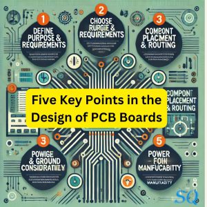
The design of a Printed Circuit Board (PCB) is a crucial step in electronic product development. A well-designed PCB ensures optimal performance, reliability, and manufacturability. Below are five essential points to consider when designing a PCB board:
Design of PCB Boards
1. Define the Purpose and Requirements
Before starting the design, clearly outline the purpose of the PCB and its requirements:
- Functionality: Understand the electronic components and their interconnections.
- Size Constraints: Determine whether the PCB needs to fit into a specific device.
- Environmental Conditions: Consider factors like temperature, humidity, and vibration that the PCB will endure.
Proper planning helps avoid costly design iterations and ensures the PCB meets all performance criteria.
2. Choose the Right Materials
The material used for the PCB significantly affects its performance. Key considerations include:
- Substrate Material: FR4 is the most common choice, but high-frequency boards may require advanced materials like Rogers.
- Copper Thickness: Affects current carrying capacity and thermal performance.
- Surface Finish: Options like HASL, ENIG, or OSP ensure solderability and longevity.
Selecting materials aligned with your design requirements ensures durability and efficiency.
3. Component Placement and Routing
Efficient component placement is critical for functionality and manufacturability:
- Logical Grouping: Place related components close to minimize signal paths and interference.
- Critical Components: Position sensitive components like oscillators away from noisy areas.
- Routing: Follow best practices like using shorter traces for high-frequency signals and minimizing vias.
Proper placement and routing reduce signal integrity issues and manufacturing complexities.
4. Power and Ground Considerations
A robust power distribution network (PDN) is essential for stable operation:
- Ground Plane: Use a dedicated ground plane to minimize noise and interference.
- Power Planes: Implement separate planes for power supplies to handle current effectively.
- Decoupling Capacitors: Strategically place capacitors near ICs to reduce power fluctuations.
A well-designed PDN enhances the reliability and performance of the PCB.
5. Design for Manufacturability (DFM) in Design of PCB Boards
Ensure the design is easy to manufacture and assemble:
- Clearances: Maintain proper spacing between components and traces to prevent short circuits.
- Test Points: Include test points for quality control during production.
- Standardization: Use industry-standard components and footprints to reduce costs and lead time.
DFM minimizes errors during manufacturing and ensures cost-effective production.
Conclusion
Designing a PCB board involves balancing functionality, manufacturability, and reliability. By focusing on these five key points—purpose, materials, placement, power, and manufacturability—you can create PCBs that meet your performance requirements and are ready for production.
our linken sqpcb.com

- long board pcb
- Flexible PCBs
- Special PCB
- Express Printed Circuit Board
- Pcb Prototype
- LED PCB
- PCB
- Printed Circuit Board
- Pcb meaning
- Pcb manufacturer
- Rigid pcb board
- Rigid Flex PCB
 Quote
Quote
 E-mail