1. Introduction to Curved PCBs
In the world of electronics, the printed circuit board has traditionally been synonymous with a flat, rigid sheet. While this configuration still dominates many applications, technological advancements have enabled the development of Curved PCBs, which break away from the two-dimensional limitation. These boards are engineered to follow a specific bend radius or curvature, allowing electronic designs to be more space-efficient, ergonomic, and visually appealing.
A Curved PCB is not simply a flat board bent into shape—it is designed from the start with its final three-dimensional geometry in mind. This means the substrate materials, copper traces, solder mask application, and component placement are all optimized to maintain functionality under bending stress.
From my perspective, what makes Curved PCBs so compelling is not just their novelty, but the way they unlock entirely new product possibilities. Flat PCBs are great for boxy, rectangular devices; curved boards enable electronics to conform to organic shapes—whether that’s a smartwatch hugging a wrist or an automotive dashboard flowing with a vehicle’s interior lines.
One key point often overlooked is that Curved PCBs can integrate both rigid and flexible zones. This hybrid design enables areas with high-density components to remain rigid for stability, while flexible or curved segments allow the board to wrap, fold, or contour to the product’s form.
Historically, such designs would have required multiple boards connected via wires or connectors—introducing potential failure points and increasing manufacturing complexity. Now, with Curved PCBs, these challenges can be reduced or eliminated entirely.
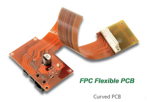
Curved PCBs
2. Evolution of PCB Technology Toward Curved PCBs
The journey toward Curved PCBs began as an extension of flexible PCB technology. In the 1980s and 1990s, manufacturers experimented with polyimide-based flexible circuits for space-saving applications in cameras, flip phones, and early laptops. These early flexible boards could bend but were not designed to hold a fixed curvature without additional mechanical support.
The first major push toward Curved PCBs came from wearable technology and automotive interior design. Wearable devices demanded compact electronics that could conform to the human body’s contours, while automotive engineers wanted lighting panels, control interfaces, and instrument clusters that followed the vehicle’s flowing lines.
From my own analysis, this shift wasn’t just driven by aesthetic or ergonomic needs—it was also an engineering necessity. As products became smaller and more integrated, designers needed to make every cubic millimeter count. A flat PCB simply left unused space in certain form factors, while Curved PCBs made better use of internal volume.
Advancements in several key areas made Curved PCBs viable at scale:
-
Material Science – Development of bend-tolerant laminates and adhesive systems that could handle repeated stress without delamination.
-
Copper Foil Technology – Introduction of rolled copper foil with superior ductility compared to electrolytic foil, reducing crack risk during bending.
-
Design Software Evolution – Modern ECAD tools now allow 3D PCB modeling, enabling designers to plan curvature and component placement with unprecedented precision.
-
Manufacturing Innovation – CNC contour cutting, precision lamination, and automated form-setting equipment now make mass production of Curved PCBs more reliable and cost-effective.
Looking at the industry’s trajectory, I believe Curved PCBs will soon be as common in certain sectors as rigid boards are today—especially in consumer electronics, automotive interiors, and medical devices.
3. Technical Foundations of Curved PCBs
The performance and reliability of Curved PCBs depend heavily on material choices, conductor properties, and thoughtful design rules. Unlike traditional rigid boards, where planar stability is the priority, curved designs must be built to withstand mechanical stress during both manufacturing and product use.
3.1 Substrate Materials for Curved PCBs
The substrate, or base layer, of a PCB determines its flexibility, heat resistance, and mechanical endurance. For Curved PCBs, materials need to balance electrical performance with bendability.
-
Polyimide (PI): A widely used flexible substrate due to its high thermal stability (up to ~260°C) and excellent mechanical endurance. It’s ideal for wearable devices and aerospace applications where durability matters.
-
Flexible Epoxy Composites: Offer good dielectric properties and are less costly than polyimide, though they may have lower heat resistance.
-
Liquid Crystal Polymer (LCP): High-frequency capable, low moisture absorption, and suitable for applications like antennas in curved surfaces.
-
Bend-Tolerant FR-4 Variants: Modified glass-reinforced epoxy resins can allow slight curvature while maintaining some rigidity for component stability.
From my engineering standpoint, the challenge isn’t just picking a material that bends—it’s ensuring it can bend reliably over years of use without developing microcracks in copper traces or delaminating under thermal cycling.
3.2 Copper Foil Selection
In Curved PCBs, copper foil choice is critical because the conductor layer must stretch slightly when bent. There are two main types:
-
Rolled Annealed (RA) Copper Foil: Produced by mechanically rolling copper into thin sheets, RA copper has elongated grain structures, making it more ductile and crack-resistant under bending.
-
Electrolytic Copper Foil (ED): Manufactured by electrodeposition on a rotating drum, ED copper is less ductile but often more affordable and suitable for mild curvatures.
Here’s the key takeaway:
Rolled copper foil is better for applications where the board must endure repeated or tight bending. Electrolytic copper foil works when the curvature is gentle, or cost is a primary concern.
(This comparison will appear again in the FAQ section for quick reader reference.)
3.3 Adhesives and Protective Layers
Curved boards also require specialized adhesives to bond copper foil to the substrate. Acrylic and epoxy adhesives are common, but thermosetting resins are gaining traction for their superior mechanical strength. Protective overlays or coverlays shield traces from abrasion, while flexible solder masks protect from oxidation without becoming brittle.
3.4 Design Software Considerations
Modern PCB CAD tools now offer 3D modeling features that allow engineers to simulate board curvature before manufacturing. This is critical for avoiding component clearance issues or stress concentration zones.
In my opinion, the best designs don’t simply “force” a flat PCB into a curve—they integrate the curvature into the layout stage. This ensures that traces follow smooth paths and avoid areas of excessive strain.
4. Manufacturing Processes for Curved PCBs
Producing Curved PCBs requires a blend of traditional PCB fabrication knowledge and specialized mechanical forming expertise. While many steps mirror those used for flat boards, the curvature introduces unique challenges in material handling, lamination, and post-processing.
4.1 Forming and Shaping Techniques for Curved PCBs
Manufacturers generally follow one of two approaches:
-
Pre-Formed Substrate Method – The base substrate is shaped before copper and components are applied. This approach reduces stress on copper traces but requires precise alignment during subsequent manufacturing steps.
-
Post-Fabrication Forming – The PCB is first fabricated as a flat flexible or semi-flexible board, then mechanically shaped into its final curve using custom molds or fixtures. This is common in wearable devices and automotive panels.
Key forming methods include:
-
Thermal Forming: The board is heated to a specific temperature to soften the substrate before bending. Once cooled, the shape is retained.
-
Cold Bending with Fixture Support: A mechanical jig applies gradual force to shape the PCB without heating. Best for gentle curves.
-
Hybrid Forming: Combines heat and controlled mechanical pressure for more complex shapes.
From my perspective, the most overlooked step in shaping is strain mapping—using simulation tools to predict where copper traces will experience the most stress and adjusting the layout accordingly.
4.2 Soldering and Component Placement on Curved PCBs
Soldering on curved surfaces introduces alignment and heat distribution issues:
-
Selective Soldering: Ideal for components located on curved segments, using localized heat to prevent thermal damage to surrounding areas.
-
Reflow Profiling Adjustments: Curved boards may heat unevenly in a standard oven, so custom reflow profiles or fixtures are used to ensure uniform solder joint quality.
-
Surface-Mount Stability: Gravity and curvature can cause components to shift during soldering—requiring temporary adhesives or custom carriers.
For complex Curved PCBs, some manufacturers place all components in flat zones and leave the bent sections as trace-only regions, avoiding soldering challenges entirely.
4.3 Quality Assurance in Curved Board Production
Quality control is more demanding for curved geometries because visual inspection and measurement require specialized tools:
-
3D Optical Inspection (AOI): Detects misalignments, solder defects, and warping.
-
Bend Fatigue Testing: Simulates repeated flexing or vibration to predict lifespan.
-
Thermal Cycling Tests: Ensures boards maintain performance after exposure to temperature extremes.
-
Electrical Continuity Checks: Verifies that traces have not cracked or delaminated due to bending stress.
In my view, a Curved PCB manufacturer’s investment in QA technology directly correlates with their ability to deliver long-lasting boards. Companies that cut corners here may face higher field failure rates—something that can severely damage a product’s reputation.
5. Advantages of Curved PCBs for Product Design
The rise of Curved PCBs is not just an engineering trend—it’s a direct response to the need for smarter, more efficient, and aesthetically appealing product designs. These boards introduce benefits that flat PCBs simply cannot match.
5.1 Space Optimization and Weight Reduction in Curved PCBs
One of the most significant advantages is the ability to maximize internal space within a product. In many modern devices, empty pockets of unused volume exist because rigid boards cannot conform to the shape of the housing. Curved PCBs solve this problem by hugging the contours of the enclosure, effectively “filling the gaps.”
For example:
-
In wearable devices like smart glasses, curved boards can wrap around the frame’s internal arc, freeing up space for additional sensors or a larger battery.
-
In automotive LED lighting, curved PCBs can follow the shape of the lens, reducing the need for multiple interconnected rigid boards.
In my analysis, space optimization directly translates into lighter devices, which is especially valuable in aerospace, drones, and portable medical devices.
5.2 Improved Ergonomics and Aesthetics in Curved PCBs
Aesthetic appeal plays a surprisingly large role in consumer purchasing decisions. Curved PCBs enable sleeker, more organic product designs. Devices feel more natural in the hand, fit better against the body, and visually differentiate themselves from “boxy” competitors.
Ergonomically, products with curves are often easier to operate. Medical handheld devices, for instance, can have curved surfaces that align with human grip patterns—while the internal PCB matches the outer shape, improving user comfort without sacrificing performance.
5.3 Electrical and Thermal Performance Benefits in Curved PCBs
At first glance, performance advantages might not seem obvious. However, the geometry of Curved PCBs can:
-
Shorten trace lengths in certain layouts, reducing signal delay and improving high-speed data transmission.
-
Distribute heat more evenly across the board surface when integrated with custom heatsink geometries.
-
Reduce the number of connectors needed, lowering signal loss and increasing reliability.
From my point of view, one overlooked benefit is reduced electromagnetic interference (EMI) in certain designs—because traces can be routed in three dimensions to naturally avoid sensitive regions.
5.4 Strategic Competitive Advantage
From a business standpoint, adopting Curved PCBs is a form factor innovation strategy. Products can stand out in crowded markets by offering a unique shape, lighter weight, and more comfortable handling. This differentiation is difficult for competitors to replicate without also investing in curved PCB design and manufacturing expertise.
In short:
-
More space → More features or larger batteries
-
Better ergonomics → Higher customer satisfaction
-
Improved performance → Stronger product reviews and brand loyalty
6. Business Perspective: How Curved PCBs Create a Competitive Edge
In today’s highly competitive electronics marketplace, product differentiation is paramount. Beyond raw performance specs, consumers and industries alike increasingly value design innovation, user experience, and reliability. Curved PCBs offer a strategic advantage by enabling these differentiators in ways that traditional flat boards cannot.
6.1 Cost–Performance Trade-Offs
While manufacturing Curved PCBs may involve higher upfront costs—due to specialized materials, tooling, and QA—these expenses are often offset by the overall product savings. Space optimization allows for smaller housings and fewer components, reducing materials and assembly labor. Fewer connectors and inter-board cables lower failure rates and warranty costs.
Moreover, the ability to integrate more features or larger batteries into the same volume can command a premium price point, improving margins. From my viewpoint, companies that consider the total cost of ownership rather than just the PCB fabrication price often realize substantial long-term value.
6.2 Market Differentiation through Form Factor Innovation
Consumers are drawn to products that not only function well but feel modern and refined. Sleek, curved designs enabled by Curved PCBs signal a premium, cutting-edge brand. In sectors like wearables, automotive interiors, and medical devices, this aesthetic and ergonomic appeal can be a deciding factor in purchase decisions.
Strategically, first movers who adopt curved PCB technology can claim leadership and innovation status, capturing market share and brand loyalty before competitors catch up.
6.3 Shorter Product Development Cycles
By leveraging modern design software and flexible manufacturing partners, companies using Curved PCBs can accelerate prototyping and iteration. This agility is crucial in fast-moving markets where time-to-market is directly tied to revenue and brand relevance.
6.4 SQ PCB as a Trusted Curved PCBs Manufacturer
When choosing a manufacturing partner for Curved PCBs, quality, experience, and innovation matter immensely. SQ PCB has established itself as a leader in precision curved board fabrication, offering:
-
Advanced thermal forming and bending capabilities
-
Expertise in selecting optimal materials and copper foils
-
Rigorous quality assurance protocols
-
Customized solutions tailored to client product requirements
By partnering with SQ PCB, businesses can reduce risk, improve yield, and bring sophisticated curved designs to market faster.
Conclusion: Why Curved PCBs Are More Than a Trend
The emergence of Curved PCBs marks a significant evolution in electronics design and manufacturing. By transcending the limitations of traditional flat boards, curved PCBs unlock new possibilities in product form, functionality, and user experience. From space optimization and improved ergonomics to enhanced electrical performance and strategic market differentiation, their advantages are multifaceted and compelling.
As industries like wearables, automotive, aerospace, and medical devices continue to demand more integrated and innovative solutions, Curved PCBs will increasingly become a standard rather than an exception. Manufacturers and designers who embrace this technology early—and collaborate with trusted partners like SQ PCB—will gain a competitive edge in delivering next-generation products.
Looking ahead, advancements in materials, AI-driven design, and additive manufacturing will further expand the potential of curved PCBs, making them essential building blocks in the future of electronics.
In my view, curved PCBs represent not just a design trend but a transformative approach that aligns engineering creativity with real-world product needs.
FAQ Section
1. What is the difference between rolled copper foil and electrolytic copper foil?
Rolled copper foil is produced by mechanically rolling copper into thin sheets, offering better surface quality and mechanical strength. Its elongated grain structure makes it more ductile and resistant to cracking when bent. Electrolytic copper foil, on the other hand, is deposited via an electrolytic process on a drum and is generally more flexible and cost-effective but less resistant to mechanical stress.
2. How durable are Curved PCBs compared to flat PCBs?
Curved PCBs are designed to withstand mechanical stresses such as bending and twisting that flat PCBs cannot endure. With appropriate materials like rolled copper foil and bend-tolerant substrates, curved PCBs maintain excellent durability and reliability, often meeting or exceeding the lifespan of flat boards in their respective applications.
3. Can Curved PCBs handle high-frequency signals?
Yes, with proper design and material selection, curved PCBs can support high-frequency signals effectively. Materials such as Liquid Crystal Polymer (LCP) and controlled impedance traces ensure signal integrity is maintained even on curved geometries.
4. What industries benefit the most from Curved PCBs?
Wearable technology, automotive interiors and lighting, aerospace instrumentation, and medical devices are primary beneficiaries. Any application requiring ergonomic form factors, space optimization, or enhanced aesthetic appeal can leverage curved PCB technology.
5. Are Curved PCBs more expensive to manufacture?
While curved PCBs can have higher upfront manufacturing costs due to specialized materials, tooling, and quality assurance, these costs are often offset by savings in overall product design, assembly simplification, and improved reliability. Additionally, as manufacturing processes mature, the cost gap continues to narrow.

- long board pcb
- Flexible PCBs
- Special PCB
- Express Printed Circuit Board
- Pcb Prototype
- LED PCB
- PCB
- Printed Circuit Board
- Pcb meaning
- Pcb manufacturer
- Rigid pcb board
- Rigid Flex PCB
 Quote
Quote
 E-mail