1. Introduction to Circuit Board Potting
1.1 What is Circuit Board Potting?
Circuit board potting is a protective process where electronic components and PCBs (Printed Circuit Boards) are encapsulated using insulating materials to shield them from environmental and mechanical damage. This technique is widely used in applications requiring high reliability, durability, and protection against harsh environments.
Printed circuit boards (PCBs) contain an electronic device’s most critical components. To protect these components from damage, electronics engineers use two main methods: PCB potting and conformal coating. Both PCB potting and conformal coating use organic polymers to protect PCBs and their associated electronic components. What are the similarities and differences between these methods, and which one is right for your electronics application? To get started, let’s find out how each technique works.
PCB potting is a method used to protect circuit boards (referred to in these contexts as the substrate) by filling a PCB enclosure with a liquid material called a potting compound or encapsulation resin. The potting compound fills the device’s housing and, in most cases, covers the entire circuit board and its components, although in some cases it can be used to pot individual components.
Potting provides excellent abrasion resistance, as well as protection against heat, chemicals, impacts and other environmental hazards. Typical potting compound materials include epoxy, polyurethane and silicone compounds.
1.2 Types of PCB Potting
Here’s a quick comparison of the most common PCB potting materials:
- Epoxy: A common and durable PCB potting material with great chemical resistance, high adhesion and many other desirable features. Its major disadvantage is the long curing time that it requires to set.
- Polyurethane: A softer and more pliable potting material that’s great for protecting sensitive connectors and other electronic components that may not tolerate more rigid materials. However, poylurethane’s moisture and heat resistance doesn’t match some other potting materials.
- Silicone: One of the most durable and flexible potting compounds, and one that’s particularly useful for applications that need to withstand extreme temperatures. Its relatively high cost, however, makes it impractical for some applications.
- PCB potting is a superior choice for applications that require high resistance to vibration, impacts, abrasion, heat and/or chemicals. In general, it’s a more durable and resilient choice that’s suitable for physically demanding applications.
- PCB potting resins offer good protection against electrical arcs, so you’ll often find PCB potting used for high-voltage electrical devices.
- PCB potting is a relatively fast process that can be done quickly and easily on an assembly line.
1.3 Importance of Circuit Board Potting in Electronics
The increasing demand for miniaturized, high-performance, and durable electronic devices has made circuit board potting an essential process in industries like automotive, aerospace, industrial automation, and consumer electronics. By applying potting compounds, manufacturers enhance moisture resistance, thermal stability, and mechanical robustness of circuit boards.
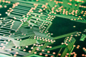
Circuit Board Potting
2. Materials Used in Circuit Board Potting
2.1 Types of Potting Compounds
Different potting materials offer unique electrical, thermal, and mechanical properties tailored for various PCB applications.
- Epoxy Resins: Provide excellent adhesion, chemical resistance, and mechanical strength. Ideal for high-temperature applications.
- Polyurethane Resins: Offer good flexibility, impact resistance, and moisture protection. Common in automotive and LED applications.
- Silicone Compounds: Known for superior heat resistance, dielectric properties, and flexibility. Suitable for high-voltage applications.
- Acrylic Compounds: Provide UV stability, fast curing, and easy removal. Often used in sensitive electronics.
2.2 Selecting the Right Circuit Board Potting Material
Choosing the correct potting compound depends on operating environment, thermal conductivity, dielectric strength, and mechanical durability. Engineers must consider:
✔ Operating temperature range
✔ Chemical and moisture exposure
✔ Mechanical stress and impact resistance
✔ Ease of application and curing time
3. Circuit Board Potting Process
3.1 Pre-Potting Preparation
Before applying potting materials, it is essential to:
- Clean the PCB to remove dust, moisture, and contaminants.
- Mask off sensitive components that should not be encapsulated.
- Check for air entrapment to prevent void formation.
3.2 Application Methods
Circuit board potting can be applied using different techniques, depending on the complexity of the PCB design:
- Manual Potting: Best for small-scale applications and prototypes.
- Automated Dispensing: Ensures precise and consistent potting in high-volume manufacturing.
- Vacuum Potting: Removes trapped air bubbles, ensuring void-free encapsulation for high-reliability PCBs.
3.3 Curing and Post-Potting Inspection
Once the compound is applied, it undergoes curing, either:
- Room-temperature curing (slow but energy-efficient)
- Heat curing (faster but requires temperature control)
- UV curing (used for specific acrylic compounds)
4. Benefits of Circuit Board Potting
Circuit board potting provides numerous advantages:
✔ Protection against moisture and contaminants
✔ Enhanced thermal dissipation for heat-sensitive components
✔ Improved mechanical stability and vibration resistance
✔ Electrical insulation and dielectric protection
✔ Longer lifespan and reliability of electronic devices
These benefits make it a crucial process in automotive electronics, industrial automation, medical devices, and aerospace systems.
5. Applications of Circuit Board Potting
5.1 Automotive Electronics
- ECUs (Electronic Control Units)
- LED lighting modules
- Battery management systems
5.2 Aerospace and Defense
- Avionics and satellite systems
- Rugged military-grade electronics
5.3 Industrial and Consumer Electronics
- Industrial control systems
- Smart home devices and IoT sensors
5.4 Medical Equipment
- Implantable medical devices
- Wearable health monitors
Each industry demands specialized potting materials with unique properties to ensure reliability, safety, and durability.
6. Challenges in Circuit Board Potting
While circuit board potting provides significant advantages, it also presents some engineering challenges:
⚠ Material shrinkage can lead to stress on PCB components.
⚠ Air bubbles and voids can reduce electrical insulation.
⚠ Long curing times can slow down production cycles.
⚠ Thermal expansion mismatches may cause material cracking.
Overcoming these challenges requires proper material selection, controlled application techniques, and optimized curing conditions.
7. Future Trends in Circuit Board Potting
7.1 Smart Potting Materials
Emerging materials with self-healing properties and nano-coatings improve PCB protection and longevity.
7.2 Advanced Automation and AI Integration
Automated AI-driven quality inspection systems ensure consistent potting applications with minimal defects.
7.3 Eco-Friendly and Sustainable Potting Solutions
With growing environmental concerns, manufacturers are developing biodegradable and low-VOC potting compounds.
7.4 High-Thermal Conductivity Potting Materials
New materials with improved heat dissipation capabilities cater to high-power electronic applications such as electric vehicles and renewable energy systems.
8. Conclusion: The Future of Circuit Board Potting
Circuit board potting remains an essential protection strategy in the electronics industry, ensuring longevity, reliability, and performance stability. With the rise of miniaturized electronics, IoT devices, and high-power PCBs, the demand for advanced potting materials and automation techniques will continue to grow.
As technology continues to evolve, the role of circuit board potting in ensuring electronic reliability and durability becomes increasingly critical. The demand for high-performance potting solutions is growing across multiple industries, including automotive, aerospace, industrial automation, medical devices, and consumer electronics. With emerging advancements in materials, application techniques, and sustainability, the future of circuit board potting is set to become even more innovative and efficient.
Enhanced Material Innovations
One of the most significant trends in the future of circuit board potting is the development of next-generation potting materials. Scientists and engineers are focusing on nano-enhanced polymers, self-healing resins, and biodegradable compounds that provide superior thermal conductivity, mechanical strength, and environmental resistance. Additionally, low-VOC (volatile organic compound) and non-toxic potting materials are being developed to meet global environmental standards.
Automation and AI Integration
The adoption of AI-driven automation in circuit board potting processes will play a pivotal role in improving efficiency, consistency, and defect detection. Automated dispensing and vacuum potting machines will ensure precision application, minimizing air bubbles and voids that could compromise PCB performance. Furthermore, real-time monitoring systems powered by AI will optimize potting quality, detecting potential defects before final production.
Sustainability and Eco-Friendly Approaches
Environmental concerns are pushing the electronics industry toward more sustainable potting solutions. Manufacturers are researching recyclable and biodegradable materials while minimizing waste and energy consumption in the potting process. Additionally, water-based potting materials and lead-free alternatives are being developed to align with global environmental regulations.
Meeting the Growing Demand for Miniaturized Electronics
As electronic devices become smaller, more complex, and more powerful, the need for high-precision potting increases. Advanced potting materials with low dielectric constants and high heat dissipation will be essential for next-generation IoT devices, wearable technology, 5G infrastructure, and AI-powered electronics.
Circuit board potting is an indispensable part of modern electronics manufacturing, ensuring long-lasting performance, protection, and reliability. As materials, processes, and technologies continue to advance, circuit board potting will remain a key factor in the success of high-performance electronics. Manufacturers that embrace innovative, automated, and sustainable potting solutions will gain a competitive edge in the ever-evolving electronics industry.

- long board pcb
- Flexible PCBs
- Special PCB
- Express Printed Circuit Board
- Pcb Prototype
- LED PCB
- PCB
- Printed Circuit Board
- Pcb meaning
- Pcb manufacturer
- Rigid pcb board
- Rigid Flex PCB
 Quote
Quote
 E-mail