Circuit Board Markings: Understanding the Importance and Standards
Circuit boards are fundamental components in nearly all modern electronic devices. These boards, also known as printed circuit boards (PCBs), are used to mechanically support and electrically connect various electronic components. To ensure the proper functioning and identify specific characteristics of each component on a PCB, various markings are added during the manufacturing process. These markings play a vital role in guiding the assembly, testing, and maintenance of electronic products. In this article, we will explore the different types of circuit board markings, their significance, and the standards that govern them.
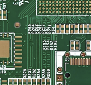
Circuit Board Markings
Types of Circuit Board Markings
Circuit board markings come in various forms, each serving a distinct purpose. Some markings are related to the electrical design, while others are related to the physical characteristics of the board. These markings provide critical information to engineers, assemblers, and technicians throughout the lifecycle of the PCB.
1. Component Markings
Component markings are perhaps the most recognizable type of PCB marking. These markings are typically used to identify the location, type, and value of individual electronic components. Common examples include:
- Resistor Markings: Resistors are commonly marked with their resistance value using a numerical code or color bands. The resistance value may be indicated directly next to the component or on the silkscreen layer of the PCB.
- Capacitor Markings: Similar to resistors, capacitors are marked with their capacitance value, voltage rating, and polarity (for electrolytic capacitors). The markings may appear next to the component or be indicated by a part number.
- Inductor Markings: Inductors, like resistors and capacitors, often carry markings that identify their inductance value, tolerance, and current rating.
- IC Markings: Integrated circuits (ICs) may feature part numbers, which are important for identifying the specific IC used. These markings are often more detailed and can include a variety of technical specifications, such as the manufacturer and series.
2. Polarity Markings
Polarity markings are used to indicate the correct orientation of components that have polarity, such as diodes, electrolytic capacitors, and some transistors. These markings are critical to prevent incorrect installation, which could lead to component damage or failure. Common polarity markings include:
- Positive (+) and Negative (-) symbols: For polarized components, a “+” or “-” sign is often placed next to the corresponding terminal on the PCB to indicate the correct orientation.
- Marking Dots or Arrows: For diodes and some other components, a dot or arrow is placed near the anode or cathode to clearly indicate the direction of current flow.
3. Footprint and Size Markings
Footprint markings refer to the specific dimensions and pad layouts that define the size and placement of components on the PCB. These markings help assembly technicians correctly place components during the manufacturing process. The footprint typically includes:
- Pads: The copper areas on the PCB where the component leads will be soldered. These pads must be properly sized and spaced to ensure the component can be installed securely.
- Silkscreen Outline: An outline of the component’s physical shape and size, typically shown on the silkscreen layer of the PCB. This provides a visual representation of where each component should be placed on the board.
4. Test Points and Debugging Markings
Test points are small pads or vias on the PCB that allow engineers and technicians to access the electrical signals at specific locations on the circuit for debugging or testing purposes. These test points are often marked with specific symbols or labels that help identify their function. For example:
- Vcc or GND: Test points may be labeled with “Vcc” or “GND” to identify voltage supply and ground connections.
- Signal Test Points: Some test points are marked with specific labels, such as “TP1” or “TP2,” which correspond to certain signals or voltages in the circuit.
5. Trace and Layer Markings
Trace markings on a PCB indicate the pathways through which electrical signals travel. These traces are often marked with a specific width and spacing to ensure proper signal integrity. In multi-layer PCBs, layer markings are used to indicate the different layers of the PCB, ensuring the correct alignment of the layers during manufacturing. These markings may include:
- Layer Numbers: In multi-layer PCBs, markings such as “Layer 1,” “Layer 2,” etc., indicate the specific layers and their respective positions within the stack-up.
- Signal Traces: Important signal traces may be labeled to indicate their specific function, such as clock signals, power traces, or ground traces.
Importance of Circuit Board Markings
The markings on a circuit board serve several critical functions throughout the design, manufacturing, and maintenance processes. Some of the key reasons for including markings on a PCB include:
1. Assembly and Manufacturing Support
Markings help guide the assembly process by clearly indicating where components should be placed, how they should be oriented, and the specific electrical characteristics of each component. This minimizes errors during assembly and ensures that components are installed correctly. The accurate placement of components also ensures that the PCB operates as intended during the final testing phase.
2. Troubleshooting and Maintenance
Circuit board markings are essential for troubleshooting and maintenance. By labeling test points, polarities, and component values, technicians can easily diagnose and fix problems in the circuit. These markings help them identify faulty components, check electrical signals, and determine the correct operation of the circuit. In the event of a failure, having proper markings can significantly reduce downtime and repair time.
3. Compliance with Standards
Circuit board markings must often comply with industry standards to ensure the PCB meets certain regulatory requirements. These standards help ensure that the PCB is safe, reliable, and meets the quality expectations of consumers and regulatory bodies. For example, components must often be labeled with specific values or tolerances to meet the requirements of organizations such as the International Electrotechnical Commission (IEC) or the Institute of Printed Circuits (IPC).
4. Component Identification and Tracking
Markings play a key role in identifying components and tracking their specifications. For example, part numbers, manufacturer information, and specific component values are marked on PCBs to help users and manufacturers quickly identify the type of component used. This is especially important in high-volume manufacturing, where consistent sourcing and compatibility between parts are critical.
Standards for Circuit Board Markings
The International PCB Association (IPC) and other regulatory bodies set out standards for circuit board markings to ensure consistency, reliability, and safety. These standards include requirements for the placement, size, and clarity of markings on the PCB. Some notable standards include:
1. IPC-2221: This standard provides guidelines for designing the PCB, including the requirements for component placement, marking specifications, and the silkscreen layer. It ensures that markings are readable and accurate, making assembly and testing easier.
2. IPC-A-600: This standard defines the acceptability of printed boards and includes specifications for marking requirements on PCBs. It ensures that the markings are properly aligned with industry expectations for quality.
3. IEC 61010: This standard, established by the International Electrotechnical Commission (IEC), outlines safety requirements for electrical equipment. It includes specifications for circuit board markings related to safety, polarity, and voltage levels.
Conclusion
Circuit board markings are not just cosmetic; they are essential for ensuring the correct assembly, testing, and maintenance of electronic devices. They provide valuable information that helps engineers, manufacturers, and technicians navigate the complexities of PCB design and operation. By adhering to industry standards and best practices, manufacturers can ensure that their PCBs are reliable, functional, and safe for use in a variety of applications. Whether it’s identifying components, indicating test points, or ensuring proper polarity, circuit board markings are indispensable for the performance and longevity of electronic systems.

- long board pcb
- Flexible PCBs
- Special PCB
- Express Printed Circuit Board
- Pcb Prototype
- LED PCB
- PCB
- Printed Circuit Board
- Pcb meaning
- Pcb manufacturer
- Rigid pcb board
- Rigid Flex PCB
 Quote
Quote
 E-mail