1: Introduction to BGA Layout
1. What is BGA Layout and Why It Matters
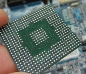
BGA Layout refers to the methodical arrangement and interconnection of Ball Grid Array (BGA) packages within a printed circuit board (PCB). BGA packages use an array of solder balls instead of leads or pins, arranged in a grid underneath the component. This architecture allows for more input/output (I/O) connections within a smaller footprint than traditional dual in-line or quad flat packages.
The importance of BGA Layout arises from the complex nature of routing signals and managing thermal dissipation through multiple layers of copper, dielectric, and via structures. A poorly executed layout can lead to parasitic inductance, excessive crosstalk, overheating, or even early failure in high-performance applications.
At its core, BGA Layout balances several constraints:
-
Escape Routing: Designing efficient paths to bring signals from the inner solder ball array to the outer PCB layer.
-
Power Integrity: Distributing clean power to each ball without voltage droop or excessive IR drop.
-
Thermal Management: Providing thermal vias and plane access to dissipate heat from the BGA pad into the copper layers or heatsinks.
-
Manufacturability: Ensuring the layout is compatible with factory capabilities like minimum trace width, solder mask registration, and via plating.
Modern applications such as high-speed processors, FPGAs, ASICs, and memory devices almost exclusively use BGAs due to their compact design and performance. Thus, mastering BGA Layout is no longer optional—it’s fundamental to successful PCB engineering.
BGA Layout
2. Historical Evolution of BGA Layout in PCB Design
The evolution of BGA Layout parallels the rapid miniaturization and power increase of integrated circuits over the past few decades. In the 1980s and early 1990s, most PCBs used leaded packages (e.g., DIP, QFP), which were easy to inspect and rework but suffered from low I/O density.
With the introduction of BGAs in the mid-1990s, designers gained access to packages that offered:
-
Higher pin counts
-
Shorter lead lengths (reducing inductance)
-
Better thermal performance due to the direct contact of the balls to the board
However, BGA packages presented a new challenge: the connections were no longer visible or accessible for probing or repair. This required:
-
X-ray inspection tools to verify solder joint integrity
-
Multilayer routing techniques with blind and buried vias
-
Controlled impedance traces to handle the growing demand for high-speed data transmission
As the technology evolved, BGAs became more complex—moving from 200-ball to over 1500-ball packages. New layout strategies were developed, including:
-
Dog-bone fanout: placing a via near each pad to bring traces to inner layers
-
Via-in-pad: embedding the via directly under the solder ball to reduce routing congestion
-
Microvias and HDI stacking: reducing layer count while increasing interconnect density
In the present era, the combination of AI computing, 5G, and ultra-low power edge devices requires not just routing capability, but signal integrity modeling, thermal simulation, and manufacturing DFM (Design for Manufacturability) awareness—all within the scope of BGA Layout.
The shift from basic signal connections to holistic performance-driven design has made the layout of BGAs a highly skilled discipline, separating average boards from mission-critical hardware.
3. Key Challenges Addressed by BGA Layout
The true power of a well-planned BGA Layout lies in its ability to address multiple technical challenges simultaneously, ensuring optimal system performance and manufacturability.
1. Signal Congestion and Escape Routing
The grid-style layout of BGAs often leads to a high density of signals in a small footprint. Routing these signals out from under the BGA pad array without causing impedance discontinuities is a major challenge.
Techniques used to mitigate this include:
-
Staggered via patterns
-
Use of multiple routing layers (e.g., Layer 3–6 exclusively for signal escape)
-
Differential pair symmetry for high-speed signals
Improper escape routing can result in length mismatches, stub reflections, or EMI emissions that degrade performance—especially in DDR, PCIe, or SerDes buses.
2. Thermal Bottlenecks
BGA components with high current draw or processing speeds generate significant heat. Without adequate thermal relief, localized hotspots may exceed solder joint limits or cause component derating.
Common BGA Layout practices to solve thermal bottlenecks include:
-
Thermal vias beneath the die-attach region
-
Embedded copper planes connected to the power/ground pads
-
Simulation-guided copper pour optimization
Factories like SQ PCB use thermal imaging to verify the layout’s effectiveness before mass production, ensuring both safety and reliability.
3. Manufacturing Alignment and Solder Integrity
Another challenge stems from the reflow process: if BGA pads are misaligned or lacking proper thermal reliefs, solder balls may not form reliable joints. This results in intermittent faults, hard-to-debug errors, or even complete device failure.
Thus, the layout must support:
-
Pad symmetry
-
Even thermal distribution
-
Solder mask defined (SMD) or non-solder mask defined (NSMD) pad strategies
BGA Layout is also critical for enabling factory testability, where access to test points, bed-of-nails fixtures, and JTAG debugging is limited due to the hidden nature of the solder joints.
4. EMI/EMC Compliance
High-frequency switching circuits in BGAs can become unintentional antennas if the layout isn’t designed with proper shielding, return path continuity, or decoupling strategies.
Good BGA Layout helps mitigate:
-
Radiated EMI by controlling return path loops
-
Common-mode noise by balanced signal layout
-
Power plane resonances by effective bypassing
4. Signal Integrity Fundamentals in BGA Layout
One of the most crucial factors in designing a reliable PCB is signal integrity (SI), and this becomes even more critical when dealing with BGA Layout. Due to the high I/O density and compact form factor of BGA packages, signal paths often need to traverse multiple layers with short clearances and tightly packed traces. This can easily lead to issues such as:
-
Reflection and ringing
-
Impedance discontinuities
-
Crosstalk between adjacent traces
-
Ground bounce and simultaneous switching noise
To mitigate these, SI-focused BGA Layout involves:
A. Controlled Impedance Routing
Controlled impedance is vital for high-speed signals such as DDR, USB 3.0, and PCIe that often originate from BGA components. Maintaining consistent trace width, spacing, and dielectric height is necessary.
-
Use of impedance calculators during layout ensures 50Ω single-ended and 100Ω differential pair impedance.
-
Via stubs should be minimized using back-drilling or via-in-pad techniques to avoid reflections.
B. Return Path Continuity
High-frequency signals seek the lowest-inductance return path, typically the reference plane beneath the signal trace. If this path is interrupted—say, by a split plane or via transition—return currents may radiate noise or induce delays.
-
In BGA Layout, designers must avoid routing signals over voids or cuts in the reference plane.
-
Stitching vias should be used to ensure continuity when changing layers.
C. Differential Pair Matching
Many BGA packages use differential signaling for robustness against EMI. Differential pairs must be routed with tight coupling and matched lengths.
-
Length mismatch tolerance is typically within 5 mils for high-speed interfaces.
-
Intra-pair and inter-pair spacing rules must be maintained even under dense BGA balls.
Ultimately, signal integrity begins at layout. Simulation software like HyperLynx or SiSoft can verify SI models post-layout, but a good BGA Layout minimizes the need for revisions. This is especially true for compact systems where BGA packages dominate the signal hierarchy.
5. Thermal Performance Considerations in BGA Layout
As BGAs pack more functions into smaller footprints, their thermal density increases significantly. Effective BGA Layout must therefore account for heat generation, dissipation paths, and environmental conditions under real-world workloads.
Without proper thermal management, excessive junction temperatures can lead to:
-
Component derating
-
Accelerated aging
-
Solder joint fatigue
-
Board warping or delamination
A. Heat Dissipation Strategies
To efficiently draw heat away from a BGA component:
-
Thermal vias should be placed under the center pad, often directly below the silicon die.
-
These vias connect to large copper pours or internal power/ground planes acting as heat spreaders.
-
Copper balancing is essential to avoid uneven etching or warping during PCB manufacturing.
Factories such as SQ PCB use simulation-driven copper stackups to ensure thermal symmetry across the board and verify that each thermal via is adequately plated and conductive.
B. Solder Joint Thermal Stress
Repeated thermal cycling can induce stress on solder joints, especially under BGAs, where expansion mismatch between PCB and component becomes significant.
-
NSMD pads (Non-solder-mask-defined) are often used to allow for better solder fillet formation and reduce stress concentration.
-
Underfill materials can be applied during assembly to mechanically reinforce solder joints and improve thermal conduction.
C. Environmental Considerations
In automotive or aerospace applications, boards may experience wide temperature swings from -40°C to 125°C or higher. BGA Layout must:
-
Place critical BGAs away from heat-sensitive passive components.
-
Use symmetrical copper patterns to reduce localized heat spots.
-
Route power planes away from heat-sensitive ICs.
Carefully designed BGA Layout ensures that even under maximum current draw, the board will not exceed thermal thresholds or create mechanical reliability risks.
6. BGA Layout via Optimization and Escape Routing
Escape routing is the process of connecting internal BGA balls to outer routing layers so they can interface with other circuit elements. Given the number of solder balls on modern BGA packages, this is one of the most constrained aspects of BGA Layout.
A. Fan-Out Patterns
The most common fan-out method is the dog-bone pattern, where a short trace exits from the ball to a nearby via. This via then brings the signal to another layer.
-
For low pin-count BGAs (<100 balls), dog-bone routing is often sufficient.
-
For high pin-count devices (>400 balls), advanced fan-out techniques such as via-in-pad or microvia stacking are required.
B. Layer Stackup Strategy
An efficient BGA Layout aligns with the board’s layer stackup. Key strategies include:
-
Reserving internal layers (e.g., L3-L6) for dense escape routing
-
Avoiding via congestion by staggering via placement between adjacent rows
-
Using blind and buried vias in HDI boards to maintain signal integrity and layer density
In HDI boards with multiple BGAs, layout planning must start early—even during schematic capture. Once the placement is fixed, escape routing options may be severely limited, making rework costly.
C. Design for Assembly and Test
Layout optimization doesn’t end at electrical performance. The layout must also be manufacturable and testable.
-
Avoid sharp via stubs that hinder solder paste flow or reflow profile consistency.
-
Place test pads on outer layers that remain accessible despite BGA obstruction.
-
Use orthogonal trace direction across adjacent layers to avoid coupling and simplify rework.
How PCB Factories Enhance Performance via BGA Layout
Leading PCB manufacturing facilities have incorporated precise BGA Layout methodologies to improve board functionality and durability. By aligning automated optical inspection (AOI) systems with ultra-fine resolution, factories detect minute layout issues early, preventing downstream yield losses.
Advanced facilities also use sequential lamination techniques, combined with micro-via laser drilling, to enhance BGA escape routing space. The thermal behavior of each BGA is simulated using in-house modeling software before production begins, allowing engineers to iteratively optimize pad distribution, via arrays, and ground plane proximity.
Reflection: The Strategic Value of Thoughtful BGA Layout
In my experience designing for both consumer and industrial systems, the most consistent differentiator between a stable board and a problematic one lies in the BGA Layout. When layout is approached not just as a placement exercise, but as a signal and thermal strategy, the return in product quality and maintenance savings is remarkable.
While software tools continue to evolve, human oversight in layout intuition remains irreplaceable. Design engineers must treat BGA Layout as both an art and a science — balancing electrical precision, manufacturability, and thermal efficiency.
Conclusion
Effective BGA Layout is essential in modern PCBs to ensure signal integrity, thermal performance, and board reliability. By understanding escape routing, via‑in‑pad vs microvia tradeoffs, layer stackup design, and thermal strategies, designers collaborate with PCB manufacturers to produce high‑quality boards. Partnering with capable fabs like SQ PCB ensures your layout rules are achievable in production.
Through thoughtful design, simulation, and manufacturability awareness, mastering BGA Layout becomes both achievable and highly beneficial for performance-critical electronics.
FAQ 1. What is the difference between rolled copper foil and electrolytic copper foil?
Rolled copper foil is produced by mechanically rolling copper into thin sheets, offering better surface quality and mechanical strength. Electrolytic copper foil is deposited via an electrolytic process and is more flexible and cost‑effective.
FAQ 2. What is via‑in‑pad and why is it used in BGA Layout?
Via‑in‑pad places the via directly inside the BGA pad to allow immediate escape routing. It’s used to save space and reduce stub length, but requires careful fabrication to avoid solder wicking.
FAQ 3. How do thermal vias improve BGA thermal performance?
Thermal vias transfer heat from the BGA package down into internal planes or heatsinks. They reduce thermal resistance and spread heat across more copper volume.
FAQ 4. Why is controlled impedance critical in BGA Layout?
Controlled impedance ensures signal edges don’t degrade or reflect, preserving signal integrity at high speeds. It requires tight control of trace width, dielectric thickness, and spacing to ground plane.
FAQ 5. How do I decide layer stackup for BGA Layout in a high‑speed design?
Start with at least two internal plane layers (GND and PWR) directly under the BGA for return path continuity. Signal layers should be adjacent for microstrip/stripline control. Match layer dielectric thickness and copper weight to impedance targets.

- long board pcb
- Flexible PCBs
- Special PCB
- Express Printed Circuit Board
- Pcb Prototype
- LED PCB
- PCB
- Printed Circuit Board
- Pcb meaning
- Pcb manufacturer
- Rigid pcb board
- Rigid Flex PCB
 Quote
Quote
 E-mail