BGA Full Name: Understanding Ball Grid Array Technology
BGA, short for Ball Grid Array, is one of the most advanced and widely used surface-mount packaging technologies in modern electronics. It provides high-density connections for integrated circuits (ICs), offering improved electrical performance, better heat dissipation, and enhanced mechanical stability compared to traditional packaging methods like Dual In-line Package (DIP) and Quad Flat Package (QFP).
BGA technology is essential in high-performance computing, telecommunications, automotive electronics, and miniaturized consumer devices. This article explores the full name and definition of BGA, its structure, advantages, manufacturing process, and applications in modern electronics.
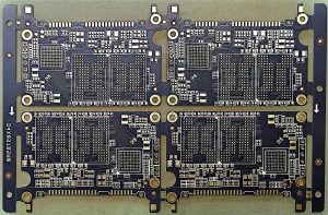
bga full name
What is BGA (Ball Grid Array)?
BGA Full Name and Definition
BGA (Ball Grid Array) is a type of surface-mount packaging (SMD) that utilizes an array of solder balls arranged in a grid pattern on the bottom of an integrated circuit (IC) package. These solder balls replace the traditional pins used in older IC packages, providing a more compact and reliable electrical connection to the PCB.
Unlike pin-based packages, where leads can bend or break, BGA uses solder balls that melt and bond to the PCB during the reflow soldering process, creating strong mechanical and electrical connections.
Structure and Components of a BGA Package
A typical BGA package consists of the following key components:
- Die (Silicon Chip) – The actual semiconductor chip where the circuits are fabricated.
- Substrate (IC Carrier) – A multilayer PCB-like structure that routes electrical connections from the die to the solder balls.
- Solder Balls – Small, uniformly spaced balls of solder that provide electrical and mechanical connections between the IC and PCB.
- Encapsulation Material – A protective resin that seals the die and substrate to prevent damage from environmental factors.
BGA Types and Variants
There are several variations of BGA packaging, each designed for specific applications:
| BGA Type | Description | Key Benefits |
|---|---|---|
| PBGA (Plastic BGA) | Uses a plastic substrate, widely used in consumer electronics. | Cost-effective, good thermal performance. |
| CBGA (Ceramic BGA) | Uses a ceramic substrate for higher reliability. | Superior thermal and mechanical properties. |
| TBGA (Tape BGA) | Uses flexible tape for interconnection. | Reduces package weight and size. |
| MicroBGA (µBGA) | Miniaturized BGA package for small devices. | Ideal for mobile phones and compact electronics. |
| FCBGA (Flip-Chip BGA) | The die is flipped and directly connected to the substrate. | Improved electrical performance and heat dissipation. |
Advantages of BGA Technology
BGA packaging has several advantages over traditional IC packaging:
1. Higher Connection Density
- BGA packages allow for more I/O connections in a smaller footprint compared to leaded packages like QFP.
- The grid arrangement of solder balls optimizes the use of available space.
2. Improved Electrical Performance
- Shorter interconnect paths reduce resistance and inductance, improving signal integrity and reducing noise.
- Lower parasitic capacitance enhances high-speed signal transmission.
3. Better Heat Dissipation
- Solder balls act as heat-conducting pathways, allowing heat to dissipate through the PCB.
- Some BGA variants include thermal vias for even better heat management.
4. Stronger Mechanical Reliability
- Unlike traditional leaded packages, BGA does not have fragile leads that can bend or break.
- The solder balls distribute stress evenly, reducing mechanical failures.
5. Simplified PCB Routing
- BGA simplifies PCB layout design because the solder ball grid provides direct contact points, eliminating complex lead routing.
BGA Manufacturing Process
The manufacturing and assembly of BGA packages involve several key steps:
1. BGA Fabrication
- The silicon die is fabricated and connected to the BGA substrate using wire bonding or flip-chip bonding.
- Solder balls are attached to the bottom of the package.
2. PCB Solder Paste Printing
- A stencil is used to apply solder paste to the PCB pads where the BGA will be placed.
3. BGA Placement
- Automated pick-and-place machines position the BGA package onto the PCB, aligning the solder balls with the pre-applied solder paste.
4. Reflow Soldering
- The PCB is heated in a reflow oven, causing the solder balls to melt and form strong electrical connections with the PCB pads.
5. Inspection and Testing
Since BGA solder joints are hidden under the package, traditional optical inspection is not possible. Instead, the following techniques are used:
- X-ray Inspection – Detects voids and defects in solder joints.
- Automated Optical Inspection (AOI) – Ensures correct component placement.
- Functional Testing – Verifies electrical performance.
Challenges and Considerations in BGA Assembly
While BGA offers many advantages, it also presents some challenges in PCB assembly and rework:
1. Difficult Rework and Repair
- BGA components cannot be manually soldered like traditional ICs.
- Specialized rework stations with hot air or infrared heating are required to remove or replace BGAs.
2. Solder Joint Voiding
- If air bubbles get trapped in the solder joints, they can create “voids” that reduce thermal and electrical conductivity.
- Optimizing the reflow profile helps minimize void formation.
3. Warpage Issues
- BGA substrates and PCBs expand at different rates during heating, causing warping and misaligned solder joints.
- Using low-stress reflow profiles and selecting materials with matched thermal expansion coefficients can reduce warpage risks.
Applications of BGA Technology
BGA is widely used in modern electronics due to its high-performance characteristics. Key applications include:
1. High-Performance Computing
- Processors (CPUs & GPUs) for servers, desktops, and gaming consoles.
- ASICs and FPGAs in data centers and AI computing.
2. Mobile and Consumer Electronics
- Smartphones, tablets, and laptops use BGA for compact designs.
- Memory chips (eMMC, DDR, NAND Flash) use BGA for high-speed data transfer.
3. Automotive Electronics
- Advanced Driver Assistance Systems (ADAS) and infotainment units use high-reliability BGA components.
- Power management ICs in electric vehicles (EVs).
4. Aerospace and Military Applications
- Ruggedized BGA packages are used in avionics, satellite systems, and defense electronics.
Conclusion
BGA (Ball Grid Array) technology has revolutionized modern electronics by enabling high-density, high-performance packaging for integrated circuits. It offers better electrical performance, improved thermal management, and superior mechanical reliability compared to traditional IC packaging.
While BGA presents challenges in rework and inspection, advancements in X-ray inspection and reflow soldering techniques have made it a widely adopted solution in industries ranging from consumer electronics to automotive and aerospace.
For high-quality BGA PCB manufacturing and assembly, Shuoqiang Electronics provides precise SMT services with advanced inspection technology. Contact us today for reliable BGA solutions!

- long board pcb
- Flexible PCBs
- Special PCB
- Express Printed Circuit Board
- Pcb Prototype
- LED PCB
- PCB
- Printed Circuit Board
- Pcb meaning
- Pcb manufacturer
- Rigid pcb board
- Rigid Flex PCB
 Quote
Quote
 E-mail