Thin PCBs (Printed Circuit Boards) are a type of PCB with a thinner thickness compared to traditional PCBs. Traditional PCBs typically range from 1.0mm (inclusive) to 2.0mm (inclusive), with the most common thicknesses being 1.0mm and 1.6mm. In contrast, thin PCBs usually have a thickness range of 0.1mm to 0.6mm (inclusive), making them ideal for compact, lightweight, and flexible electronic applications.
With the growing demand for miniaturized devices, thin-PCBs are widely used in wearable technology, medical electronics, smartphones, aerospace systems, and flexible circuits. These ultra-thin boards not only provide space efficiency, lightweight design, and enhanced flexibility but also present many unique manufacturing and handling challenges.
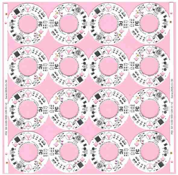
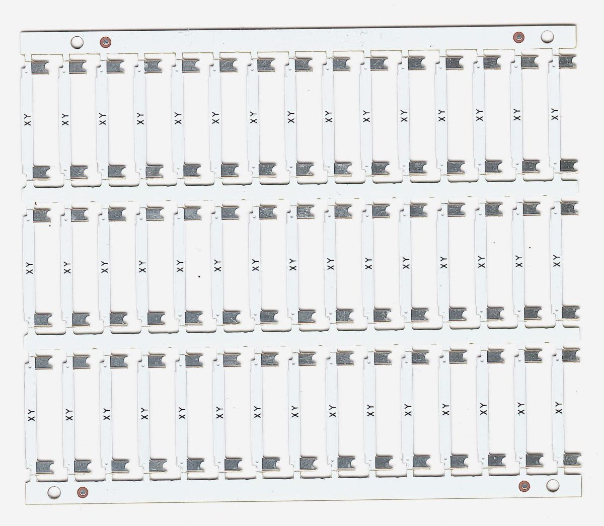
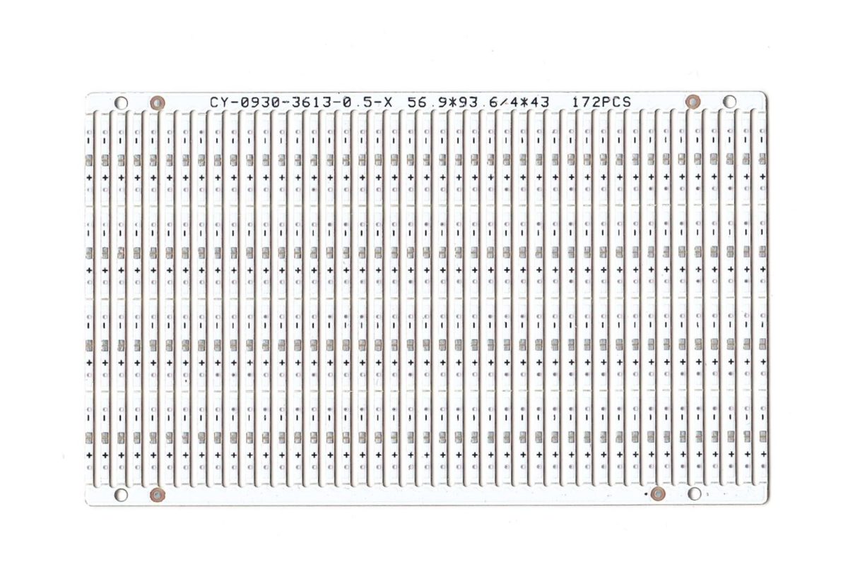
[caption id="attachment_2930" align="alignnone" width="300"] Thin PCB[/caption]
Lightweight and Compact Design
Thin PCBs are significantly lighter and more compact, making them perfect for space-constrained portable devices. This feature is particularly important in aerospace and medical industries, where reducing overall device weight is a priority.
High Flexibility and Bendability
Many thin-PCBs are designed as flexible PCBs (FPCs), allowing them to bend and conform to complex shapes. This makes them suitable for foldable displays, flexible electronics, and automotive systems.
Improved Thermal Management
Due to their lower material density, thin-PCBs dissipate heat more effectively, reducing the risk of overheating in high-power electronic components. Metal-based thin PCBs, such as aluminum-based ones, are commonly used in LED and power electronics due to their excellent thermal conductivity.
High-Density Component Integration
Despite their reduced thickness, thin PCBs still support fine-pitch components, microvias, and advanced interconnect technologies, enabling the miniaturization of electronic devices and high circuit density.
Thin-PCBs come in various thickness options, depending on the application requirements:
Ultra-Thin: 0.1mm – 0.4mm (Used in medical sensors, RFID tags, and flexible circuits)
Standard Thin: 0.5mm – 1.0mm (Common in mobile devices, consumer electronics, and aerospace systems)
Thin Rigid PCBs: 0.6mm – 1.2mm (Used in compact automotive control systems and industrial applications)
The choice of thickness depends on the mechanical strength, flexibility, and electrical performance needs.
Due to their compact and lightweight nature, thin PCBs are widely used across various industries:
Wearable Technology
Smartwatches, fitness trackers, and augmented reality (AR) glasses leverage the flexibility and space-saving advantages of thin PCBs.
Smartphones and Tablets
Thin-PCBs help reduce the device thickness, making smartphones and tablets slimmer and lighter.
Medical Devices
Thin-PCBs are widely used in implantable sensors, diagnostic tools, and flexible electrodes due to their precise performance and biocompatibility.
Aerospace and Defense
Thin-PCBs are used in satellite communication systems, aircraft control modules, and radar systems, reducing device weight, enhancing fuel efficiency, and improving overall performance.
Automotive Electronics
Thin-PCBs are used in adaptive lighting systems, heads-up displays (HUD), and compact control units in modern vehicles.
Flexible and Foldable Electronics
Thin-PCBs are essential for developing flexible OLED displays, rollable screens, and next-generation consumer electronics.
The production of thin-PCBs requires precise processes and equipment and faces several unique challenges:
Handling and Warping Issues
Thin-PCBs are prone to bending and warping, making their assembly and soldering more challenging. To overcome this, panel reinforcement techniques are often employed during manufacturing.
Precision Drilling and Via Formation
Ultra-thin PCBs require precision laser drilling to create microvias, as mechanical drilling can damage fragile substrates.
Thermal Stress and Expansion Management
Thin PCBs have a higher coefficient of thermal expansion (CTE), which can cause dimensional instability during soldering. The selection of high-Tg FR-4 or polyimide materials can help minimize the effects of thermal expansion.
Complexity in Component Assembly
Assembling fine-pitch components on thin PCBs requires advanced surface mount technology (SMT). Careful optimization of the reflow soldering process is critical to avoid damaging fragile substrates.
Cost Considerations
Manufacturing high-precision thin-PCBs requires precise etching, fine-pitch alignment, and the use of flexible materials, which makes them more expensive. However, the performance and miniaturization benefits often justify the higher costs in high-tech applications.
Nevertheless, SQPCB successfully solves these challenges. SQPCB can handle thin-PCBs with a minimum thickness of 0.1mm and uses chemical treatment instead of traditional brushing methods to prevent bending and wrinkling issues. Furthermore, SQPCB employs specialized electroplating fixtures to ensure that thin PCBs remain stable and intact during the electroplating process, avoiding bending or breakage.
What is the main difference between thin-PCBs and standard PCBs?
Thin PCBs are typically under 1.0mm thick, whereas standard PCBs range from 1.6mm to 3.2mm in thickness. Thin PCBs are ideal for applications that require higher integration, lighter weight, and flexible designs.
What are the common applications of thin-PCBs?
Thin PCBs are widely used in industries like smartphones, wearable technology, medical devices, automotive electronics, aerospace, and flexible electronics. They are especially suited for devices that need high integration, space-saving, and lightweight designs.
Are thin PCBs more expensive to manufacture?
Since thin PCBs require more precise manufacturing processes and materials, their production cost is typically higher than standard PCBs. However, in high-tech applications, the performance benefits of thin PCBs often justify the additional cost.
What advantages does SQPCB offer in manufacturing thin PCBs?
SQPCB uses chemical treatment instead of traditional brushing methods, preventing bending and wrinkling during surface processing. Additionally, SQPCB employs specialized electroplating fixtures, ensuring the stability and integrity of thin PCBs during electroplating.
How do I choose the thickness for a thin-PCB?
The thickness of a thin-PCB depends on the specific application requirements. For designs that need higher flexibility and ultra-thin characteristics, you can choose ultra-thin PCBs (0.1mm to 0.4mm). For most consumer electronics and mobile devices, standard thin PCBs (0.5mm to 1.0mm) are more common.

 Quote
Quote
 E-mail