Nickel-Palladium-Gold (NiPdAu): The Direct Bonding Finish for Semiconductor Packages
Introduction
As semiconductor packages continue to shrink while performance expectations continue to rise, surface finish technology has become one of the most critical factors in advanced PCB manufacturing and packaging reliability. Traditional surface finishes such as HASL, ENIG, OSP, and immersion silver each provide distinct advantages, but modern semiconductor packaging increasingly demands finishes capable of supporting ultra-fine pitch interconnections, direct wire bonding, high-frequency transmission, thermal cycling reliability, and long-term corrosion resistance. Among the available technologies, Nickel-Palladium-Gold (NiPdAu) has emerged as one of the most sophisticated and performance-oriented solutions for advanced semiconductor packaging applications.
Nickel-Palladium-Gold is widely recognized as a premium surface finish that combines the mechanical robustness of nickel, the diffusion barrier properties of palladium, and the oxidation resistance of gold. This multilayer finish has become especially important in semiconductor substrates, IC package carriers, automotive electronics, aerospace modules, RF devices, and high-reliability computing hardware. Unlike conventional ENIG finishes, NiPdAu is specifically optimized for direct bonding applications and fine interconnect reliability, making it particularly attractive for modern semiconductor assembly processes.
In recent years, the electronics industry has experienced rapid evolution driven by artificial intelligence hardware, 5G communications, electric vehicles, industrial automation, and advanced computing systems. These applications require packaging solutions that can handle higher current densities, faster signal speeds, and more compact layouts without compromising reliability. Surface finish selection therefore becomes more than a simple manufacturing choice; it becomes a strategic engineering decision that influences electrical performance, manufacturability, assembly yield, and product lifetime.
From my perspective, NiPdAu represents more than just another surface finish technology. It reflects how PCB manufacturing is gradually integrating with semiconductor-level engineering requirements. The traditional boundary between PCB fabrication and semiconductor packaging is becoming increasingly blurred. In this transition, NiPdAu serves as a bridge technology that enables PCB manufacturers to meet the demands previously associated only with semiconductor substrate fabrication.
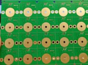
Nickel-Palladium-Gold
Nickel-Palladium-Gold Definition and Core Structure
Nickel-Palladium-Gold Layer Architecture
Nickel-Palladium-Gold is a multilayer metallic surface finish composed of three primary deposition layers:
- Electroless nickel layer
- Electroless or immersion palladium layer
- Thin immersion gold layer
Each metallic layer serves a specific engineering purpose within the total finish system.
The nickel layer functions primarily as a diffusion barrier and mechanical support structure. It prevents copper migration into the upper layers while providing hardness and structural integrity. Typical nickel thickness ranges from 3 µm to 6 µm depending on the application requirements.
The palladium layer acts as an intermediate barrier that protects nickel from corrosion and oxidation. Palladium significantly improves wire bonding performance and reduces the risk of nickel-related reliability issues. Typical palladium thickness ranges between 0.05 µm and 0.15 µm.
The gold layer serves primarily as oxidation protection during storage and assembly. Unlike thick hard gold plating, the gold in NiPdAu is extremely thin, usually between 0.03 µm and 0.08 µm. Because the gold is thin, the process remains economically manageable while still providing excellent solderability and bondability.
This multilayer combination enables NiPdAu to support both solder assembly and direct wire bonding simultaneously, which is one of its greatest advantages in semiconductor packaging applications.
Nickel-Palladium-Gold Chemical Principles
The effectiveness of NiPdAu depends heavily on electrochemical compatibility between the deposited layers. Nickel naturally forms oxides when exposed to air, which can reduce bonding reliability. Palladium prevents this oxidation from occurring by serving as a protective intermediate layer.
Gold alone cannot fully solve nickel corrosion problems because extremely thin gold layers may contain microscopic pores. These pores allow environmental contaminants to reach the nickel surface. Palladium acts as an additional corrosion-resistant barrier that dramatically improves reliability under harsh operating conditions.
The chemistry behind NiPdAu deposition is highly controlled. Bath contamination, pH stability, reducing agents, temperature management, and metallic ion concentration all directly affect coating uniformity and long-term reliability.
In my opinion, one of the most fascinating aspects of NiPdAu technology is how microscopic metallurgical interactions determine the reliability of billion-dollar electronic systems. Tiny variations in atomic diffusion behavior can eventually influence signal integrity, package cracking, or bonding failures years later.
Nickel-Palladium-Gold Versus ENIG
NiPdAu is often compared with ENIG because both use electroless nickel and immersion gold structures. However, the addition of palladium fundamentally changes the finish behavior.
ENIG structure:
Copper → Nickel → Gold
NiPdAu structure:
Copper → Nickel → Palladium → Gold
The palladium layer offers several important improvements:
- Better wire bonding performance
- Reduced black pad risk
- Improved corrosion resistance
- Enhanced thermal cycling reliability
- Better compatibility with aluminum wire bonding
- Lower nickel oxidation exposure
Although ENIG remains extremely popular for standard PCB applications, NiPdAu is generally preferred for semiconductor package substrates where direct bonding reliability is critical.
Nickel-Palladium-Gold Manufacturing Processes
Nickel-Palladium-Gold Pretreatment Procedures
Successful NiPdAu deposition begins with extremely rigorous surface preparation. Copper contamination, oxidation, oils, fingerprints, and particulate residues can all cause plating defects.
The pretreatment process typically includes:
- Degreasing
- Micro-etching
- Acid cleaning
- Water rinsing
- Surface activation
Semiconductor package substrates require much tighter contamination control than ordinary PCBs. Even microscopic residues may create non-wetting defects or bonding reliability issues.
Modern manufacturing facilities therefore use automated chemical dosing systems, inline filtration, conductivity monitoring, and statistical process control throughout the pretreatment stage.
Nickel-Palladium-Gold Nickel Deposition
The electroless nickel process is autocatalytic. Unlike electrolytic plating, electroless deposition does not require external electrical current.
Key parameters include:
- Nickel ion concentration
- Hypophosphite reducing agent concentration
- Bath temperature
- pH value
- Agitation uniformity
- Deposition rate control
Phosphorus content within the nickel layer strongly affects mechanical and corrosion properties. High-phosphorus nickel offers superior corrosion resistance, while lower-phosphorus nickel may provide different hardness characteristics.
Nickel uniformity is extremely important because thickness variation can affect impedance consistency and bonding quality.
Nickel-Palladium-Gold Palladium Deposition
The palladium layer is one of the defining characteristics of NiPdAu technology.
Palladium serves multiple purposes:
- Nickel protection
- Bonding enhancement
- Corrosion reduction
- Diffusion control
The deposition thickness must be carefully optimized. Excessively thin palladium may not provide sufficient barrier protection, while overly thick palladium increases cost significantly.
Because palladium is a precious metal with volatile market pricing, manufacturers continuously optimize deposition efficiency to reduce waste while maintaining reliability.
Nickel-Palladium-Gold Gold Deposition
The immersion gold layer is intentionally thin because its primary role is oxidation prevention rather than mechanical wear resistance.
Gold thickness uniformity is especially important for semiconductor bonding applications. Inconsistent gold deposition may produce variable bond pull strengths during assembly.
The gold process also requires precise contamination control because impurities can interfere with ultrasonic wire bonding processes.
Nickel-Palladium-Gold Advantages and Limitations
| Advantages | Limitations |
| Excellent wire bonding compatibility | Higher manufacturing cost |
| Superior corrosion resistance | Complex process control requirements |
| Strong thermal cycling reliability | Precious metal price fluctuations |
| Excellent flatness for fine-pitch assembly | Higher inspection and qualification costs |
| Reduced black pad risk compared with ENIG | Requires advanced manufacturing capability |
| Suitable for semiconductor packaging | More demanding chemical maintenance |
Conclusion
Nickel-Palladium-Gold has become one of the most important surface finish technologies in advanced semiconductor packaging and high-reliability PCB manufacturing. By combining nickel, palladium, and gold into a carefully engineered multilayer structure, NiPdAu delivers outstanding wire bonding compatibility, corrosion resistance, thermal reliability, and electrical stability.
Although the technology introduces higher material and manufacturing costs compared with standard PCB finishes, its performance advantages often justify the investment in demanding applications such as automotive electronics, aerospace systems, AI accelerators, RF modules, and semiconductor package substrates.
The addition of palladium fundamentally improves the limitations associated with traditional nickel-gold finishes, especially in direct bonding applications. As semiconductor packaging continues evolving toward smaller geometries, higher frequencies, and greater integration density, the importance of highly reliable surface finishes will only continue growing.
From my perspective, NiPdAu represents a broader transformation within the electronics industry. Surface finishing is no longer merely a protective coating process; it has become a critical enabler of next-generation semiconductor performance. Future advances in AI hardware, chiplet architectures, heterogeneous integration, and advanced packaging will likely push NiPdAu technology toward even greater precision and sophistication.
Ultimately, the success of NiPdAu depends not only on chemistry but also on manufacturing discipline, process control, supplier capability, and engineering collaboration. Companies that can master these interconnected factors will be best positioned to support the next era of semiconductor innovation.
FAQ
1. What is the difference between Nickel-Palladium-Gold and ENIG?
Nickel-Palladium-Gold includes an additional palladium layer between the nickel and gold layers, while ENIG uses only nickel and gold. The palladium layer improves corrosion resistance, wire bonding reliability, and protection against nickel oxidation. NiPdAu is therefore more suitable for advanced semiconductor packaging and direct bonding applications.
2. Why is Nickel-Palladium-Gold commonly used in semiconductor packages?
NiPdAu provides excellent wire bonding performance, stable solderability, strong corrosion resistance, and high thermal reliability. These characteristics make it ideal for semiconductor substrates, fine-pitch IC packages, automotive electronics, and high-frequency devices.
3. Does Nickel-Palladium-Gold increase PCB manufacturing cost?
Yes. NiPdAu is more expensive than many standard surface finishes because it uses precious metals such as palladium and gold and requires highly controlled manufacturing processes. However, the improved reliability often justifies the higher cost in mission-critical electronics.
4. What types of wire bonding are compatible with Nickel-Palladium-Gold?
NiPdAu is compatible with gold wire bonding, copper wire bonding, and aluminum wire bonding. This flexibility makes it highly attractive for advanced semiconductor assembly processes.
5. How does Nickel-Palladium-Gold affect PCB performance?
NiPdAu improves PCB performance by enhancing corrosion resistance, electrical stability, solderability, bonding reliability, and thermal cycling durability. It also supports smoother surfaces that benefit high-speed and RF signal transmission.

- long board pcb
- Flexible PCBs
- Special PCB
- Express Printed Circuit Board
- Pcb Prototype
- LED PCB
- PCB
- Printed Circuit Board
- Pcb meaning
- Pcb manufacturer
- Rigid pcb board
- Rigid Flex PCB
 Quote
Quote
 E-mail