Selective ENIG: Combining Gold Fingers with OSP on the Same Board
Introduction
Modern electronic products are moving toward higher integration, faster signal transmission, smaller form factors, and stricter cost targets. As a result, PCB manufacturers and design engineers must continuously optimize not only circuit layout and material selection, but also surface finish strategies. One increasingly popular solution is Selective ENIG, a hybrid surface treatment approach that applies ENIG to specific functional areas such as gold fingers while using OSP on solderable regions of the same PCB.
This manufacturing strategy allows designers to combine durability, conductivity, solderability, and cost optimization in a single board design. Instead of applying expensive gold finishing across the entire PCB, manufacturers selectively protect edge connectors and high-wear contacts with ENIG while maintaining lower-cost OSP treatment on assembly pads. This creates an efficient balance between electrical performance and manufacturing economics.
As electronic systems evolve toward high-speed computing, automotive electronics, industrial automation, telecommunications infrastructure, and AI hardware platforms, the demand for selective surface finishing continues to increase. Engineers no longer evaluate PCB surface finish solely from the perspective of solderability. Instead, reliability under mechanical insertion cycles, corrosion resistance, impedance stability, thermal endurance, and assembly compatibility all become critical considerations.
In many modern designs, the PCB itself becomes part of the electromechanical interface. Edge connectors frequently interact with sockets, card slots, or docking systems. These insertion interfaces require hard, wear-resistant metallic surfaces capable of surviving repeated friction without degradation. At the same time, the majority of assembly pads only require good solderability during SMT assembly and do not benefit from expensive noble-metal coatings. This mismatch in functional requirements is precisely why selective surface finish technology has gained significant traction.
From my perspective, Selective ENIG represents more than a process innovation. It reflects a broader engineering philosophy: applying high-performance materials only where necessary while maximizing efficiency elsewhere. This concept aligns strongly with modern manufacturing trends focused on sustainability, cost control, and functional optimization.
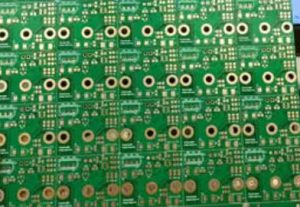
Combining Gold Fingers with OSP
Understanding Combining Gold Fingers with OSP
What Is Combining Gold Fingers with OSP?
Combining Gold Fingers with OSP refers to a hybrid PCB surface finishing method in which different surface treatments are applied selectively across the same printed circuit board. Typically, ENIG or hard gold plating is used on edge connectors or gold finger regions, while Organic Solderability Preservative (OSP) is applied to soldering pads and component assembly areas.
This approach enables manufacturers to achieve multiple objectives simultaneously:
- High wear resistance on connector contacts
- Excellent solderability for SMT assembly
- Lower overall manufacturing cost
- Reduced precious metal consumption
- Improved production flexibility
- Better optimization of functional regions
Gold fingers are conductive contact pads located on PCB edges that interface with sockets or connectors. These regions experience repeated mechanical insertion and removal cycles. Because of this mechanical stress, they require highly durable metallic finishes such as hard gold or ENIG.
OSP, by contrast, is an organic coating designed primarily to protect exposed copper from oxidation before soldering. It creates an ultra-flat surface ideal for fine-pitch SMT assembly while maintaining relatively low cost.
Selective ENIG technology merges these two finishing philosophies into one board.
Why Combining Gold Fingers with OSP Matters in Modern Electronics
The evolution of modern electronics has dramatically changed PCB requirements. Earlier PCB generations often used single-finish strategies because designs were relatively simple. However, today’s electronic systems contain multiple functional zones with completely different reliability demands.
For example:
| PCB Area | Functional Requirement | Preferred Finish |
|---|---|---|
| Gold Fingers | Wear resistance | ENIG / Hard Gold |
| BGA Pads | Flat solderable surface | OSP |
| Fine-Pitch SMT Pads | Oxidation protection | OSP |
| High-Speed Contacts | Stable conductivity | ENIG |
| Connector Interfaces | Corrosion resistance | Gold |
Applying gold finish to the entire PCB may improve durability, but it dramatically increases cost. Conversely, using OSP everywhere reduces cost but cannot withstand connector wear. Selective ENIG solves this contradiction elegantly.
In my opinion, the importance of this technology lies in functional specialization. Instead of treating the entire PCB uniformly, manufacturers now engineer surface finishes according to local operational demands.
Combining Gold Fingers with OSP and Cost Optimization
Combining Gold Fingers with OSP Reduces Precious Metal Consumption
Gold is expensive. Applying ENIG or hard gold across an entire PCB substantially increases production cost.
Selective finishing reduces noble-metal usage dramatically.
Example comparison:
| Surface Finish Strategy | Relative Cost |
|---|---|
| Full ENIG | High |
| Full Hard Gold | Very High |
| Full OSP | Low |
| Selective ENIG + OSP | Medium |
Selective finishing provides an effective balance between performance and cost.
For large-volume manufacturing, the savings become substantial.
Combining Gold Fingers with OSP and Fine-Pitch BGA Reliability
Modern electronic systems increasingly depend on ultra-fine-pitch BGA packages.
Challenges include:
- Smaller solder volumes
- Tighter spacing
- Higher thermal density
- Reduced process margins
OSP’s ultra-flat surface profile becomes highly advantageous in these conditions.
Compared with HASL finishes, OSP minimizes:
- Solder bridging
- Coplanarity variation
- Uneven solder joints
This directly improves assembly yield rates.
Meanwhile, selective ENIG protects connector regions without interfering with BGA assembly performance.
This combination is especially valuable for:
- Networking equipment
- AI modules
- Medical electronics
- Aerospace computing systems
Combining Gold Fingers with OSP and Reliability Testing
Combining Gold Fingers with OSP Through Thermal Cycling Evaluation
Reliability validation remains essential for hybrid surface-finish PCBs.
Manufacturers commonly perform:
- Thermal cycling tests
- Humidity exposure testing
- Salt spray testing
- Insertion cycle testing
- Solderability evaluation
Thermal cycling tests simulate repeated expansion and contraction under changing temperatures.
Potential failure mechanisms include:
- Nickel cracking
- Gold delamination
- OSP degradation
- Contact resistance increase
Reliable process control minimizes these risks significantly.
Combining Gold Fingers with OSP and Contact Resistance Stability
Gold fingers must maintain stable electrical contact over extended operational life.
Contact resistance testing often evaluates:
- Initial resistance
- Resistance after insertion cycles
- Resistance after environmental aging
- Resistance under vibration
High-quality ENIG or hard gold finishes maintain low resistance even after prolonged mechanical stress.
Poor plating quality, however, can lead to:
- Surface wear
- Oxidation
- Increased resistance
- Intermittent failures
This is why precision plating control becomes essential in selective finishing manufacturing.
Combining Gold Fingers with OSP and PCB Material Compatibility
Combining Gold Fingers with OSP on High-Tg Materials
Many advanced PCBs now utilize high-Tg laminates for improved thermal stability.
These materials support:
- Lead-free assembly
- High-temperature operation
- Reduced warpage
- Improved reliability
Selective ENIG processes must remain compatible with these substrates.
Challenges include:
- Differential thermal expansion
- Surface adhesion consistency
- Resin interaction during plating
Proper process engineering ensures stable finish adhesion across varying laminate systems.
Combining Gold Fingers with OSP and Low-Loss Materials
High-frequency applications increasingly rely on low-loss dielectric materials.
Examples include:
- Rogers laminates
- Megtron series
- PTFE composites
- Advanced hydrocarbon ceramics
These materials require highly controlled manufacturing conditions.
Surface finish roughness directly affects conductor loss at high frequencies.
OSP generally preserves smoother copper surfaces compared with thicker metallic finishes, which can improve RF performance in certain applications.
Meanwhile, selective gold plating protects connector interfaces where durability remains essential.
Conclusion
Selective ENIG technology represents an important evolution in PCB surface engineering. By combining durable gold-finished connector regions with cost-effective OSP-coated solderable areas, manufacturers achieve an optimized balance between reliability, performance, and cost efficiency.
This hybrid approach addresses multiple challenges simultaneously:
- Connector wear resistance
- Fine-pitch solderability
- Signal integrity
- Material cost control
- Environmental sustainability
As modern electronics continue demanding higher density, faster signaling, and lower manufacturing costs, the importance of selective surface finishing will only grow stronger.
From consumer electronics to automotive systems, telecommunications infrastructure, AI computing hardware, and industrial automation, Combining Gold Fingers with OSP offers a practical and forward-looking solution for advanced PCB manufacturing.
The continued development of selective finishing technologies will likely shape the next generation of high-performance PCB fabrication strategies.
FAQ
1. What is the difference between ENIG and OSP in PCB manufacturing?
ENIG uses electroless nickel and immersion gold to create a durable, corrosion-resistant metallic surface. OSP uses an organic coating to protect copper before soldering. ENIG offers better wear resistance and connector reliability, while OSP is more cost-effective and provides excellent SMT solderability.
2. Why are gold fingers usually plated with gold instead of OSP?
Gold fingers experience repeated mechanical insertion and removal cycles. OSP coatings wear away quickly under friction, while gold plating maintains conductivity, corrosion resistance, and low contact resistance over long operational lifespans.
3. What are the main advantages of selective ENIG technology?
Selective ENIG provides:
- Lower manufacturing cost
- Reduced gold usage
- Excellent solderability
- High connector durability
- Better optimization of PCB functional areas
It combines the strengths of both ENIG and OSP within a single PCB.
4. Does Combining Gold Fingers with OSP improve signal integrity?
Yes. Gold-plated connectors provide stable electrical contact and reduced oxidation, which helps maintain signal integrity. OSP-coated soldering regions also preserve flat copper surfaces that support high-quality SMT assembly and stable electrical performance.
5. Is selective ENIG suitable for automotive and industrial applications?
Yes. Automotive and industrial systems often require both durable connector interfaces and cost-effective assembly surfaces. Selective ENIG is widely used in:
- Automotive ECUs
- Industrial controllers
- Telecom backplanes
- High-speed computing systems
because it balances reliability and manufacturing economics.

- long board pcb
- Flexible PCBs
- Special PCB
- Express Printed Circuit Board
- Pcb Prototype
- LED PCB
- PCB
- Printed Circuit Board
- Pcb meaning
- Pcb manufacturer
- Rigid pcb board
- Rigid Flex PCB
 Quote
Quote
 E-mail