Gold Fingers in PCB: Design, Plating, and Manufacturing Best Practices
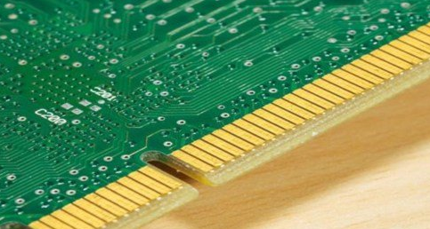
In high-reliability electronic systems, gold fingers are not just a finishing touch—they are essential. Acting as the edge connectors between a PCB and an external device or motherboard, gold fingers play a pivotal role in ensuring durable, low-resistance, and high-cycle connections.
But here’s the kicker…
Not all gold fingers are created equal. Their performance depends heavily on the PCB manufacturer’s plating quality, mask clearance precision, and equipment accuracy. In this article, we explore what gold fingers are, why they matter, and how to PCB manufacture them right.

Gold Fingers
1. What Are Gold Fingers in PCBs?
● Gold fingers are the gold-plated connectors located along the edge of a PCB.
● They enable the board to plug into other components (e.g., memory slots, backplanes, interface connectors).
● Typically found in RAM modules, PCIe cards, graphics cards, and industrial control boards.
2. Why Use Gold Plating for Connectors?
● Durability: Gold resists oxidation and corrosion better than most metals.
● Conductivity: Offers excellent electrical conductivity with low contact resistance.
● Wear Resistance: Hard gold plating (electroplated) withstands frequent mating cycles.
3. Types of Gold Plating on Gold Fingers
| Type | Process | Thickness Range | Application |
|---|---|---|---|
| ENIG (Electroless Nickel Immersion Gold) | Chemical deposition | 0.03–0.1 μm (gold layer) | Good for signal pads, not recommended for gold fingers |
| Electroplated Hard Gold | Electroplating with nickel barrier | 0.76–1.27 μm (or more) | Preferred for gold fingers due to durability |
Important: Only hard gold is used for gold fingers. ENIG is too soft for repeated insertions.
4. Design Considerations for Gold Fingers
● Plating Thickness: IPC recommends 30–50 μin gold over 100–150 μin nickel.
● Chamfering Angle: Usually 30° or 45° to aid insertion.
● Length Tolerance: ±0.13mm typical.
● Mask Clearance: No solder mask or silkscreen on fingers; 1mm clearance standard.
● Number of Insertions: Up to 1,000 cycles depending on thickness & finish.
5. Chamfering Process
Gold fingers are usually beveled (chamfered) after board routing and before plating to ensure:
● Smooth connector insertion
● No mechanical interference
● Proper gold plating coverage on edge tips
6. IPC Standards for Gold Fingers
Gold finger production is typically governed by:
● IPC-6012: Qualification and performance specification for rigid PCBs
● IPC-A-600: Acceptability of printed boards (Class 2 for commercial, Class 3 for aerospace/medical)
Complying with IPC Class 3 ensures the highest level of mechanical durability, plating quality, and cleanliness.
7. PCB Manufacturing Requirements for Gold Fingers
To produce high-quality gold fingers, strict controls are needed in:
● Mask clearance alignment
● Plating bath control
● AOI for pad size and position
● Edge smoothness after routing and chamfering
This is where equipment matters.
8. Why Choose SQPCB for Gold Finger PCBs?
SQPCB integrates LDI inline exposure for trace, solder mask, and legend layers. Here’s why it matters:
Eliminates film distortion and alignment errors common in old-generation exposure machines
Prevents scratch marks, foreign debris, and rework, especially around precision pads like gold fingers
Enhances solder mask glossiness, improving both aesthetics and performance
Furthermore, SQPCB operates with in-house lamination, HASL, and ENIG lines, ensuring complete control over quality and delivery timelines.
9. Use Cases and Applications
Gold fingers are essential in:
● High-speed interface cards (e.g., PCIe, SATA, USB)
● Memory modules (DDR, SSD)
● Industrial PLCs and backplanes
● Custom embedded systems and military electronics
These applications demand both durability and high signal integrity.
10. Challenges in Gold Finger Manufacturing
● Achieving tight plating thickness tolerance
● Preventing edge burns or nickel underplating
● Ensuring solder mask peel-back from the gold pad edges
● Avoiding mechanical damage during V-cut and routing
11. Secondary SQPCB Recommendation
At SQPCB, we don’t just plate gold—we engineer reliability. With:
LDI automatic exposure for track, solder mask, and legend layers
In-house ENIG and HASL lines
100% AOI and electrical testing
Expert engineering review during DFM
We ensure your gold finger PCBs meet the highest industrial expectations—whether you’re building a rugged military system or a consumer-grade expansion card.
12. Future Trends in Gold-Finger Technology
● Selective hard gold plating to reduce cost while maintaining function
● Nanogold plating techniques to reduce material usage
● Integrated edge connectors with embedded capacitive/EMI filtering
● Low-profile edge designs for ultra-slim devices
FAQs About PCB Gold Fingers
Q1: What is the standard gold thickness for PCB gold-fingers?
A: IPC recommends 30–50 μin (0.76–1.27 μm) of hard gold over 100–150 μin (2.54–3.81 μm) of nickel for durability.
Q2: Can ENIG be used instead of hard gold for fingers?
A: No. ENIG is too soft and will wear out quickly under repeated mating cycles. Only hard gold (electroplated) is suitable.
Q3: Why is chamfering necessary for gold-fingers?
A: Chamfering ensures smooth connector insertion, prevents contact wear, and improves plating consistency along the edges.
Q4: How do you avoid solder mask defects near gold-fingers?
A: Keep a 1mm clearance from the solder mask and legend layers. SQPCB’s LDI exposure ensures accurate edge alignment.
Q5: Can SQPCB handle high-volume or prototype gold-finger PCBs?
A: Absolutely. SQPCB supports both small batches and mass production, with controlled in-house processes and quick-turn options.
- long board pcb
- Flexible PCBs
- Special PCB
- Express Printed Circuit Board
- Pcb Prototype
- LED PCB
- PCB
- Printed Circuit Board
- Pcb meaning
- Pcb manufacturer
- Rigid pcb board
- Rigid Flex PCB

 Quote
Quote
 E-mail