Introduction to Laser Soldering in High-Density PCBs
In recent years, the electronics industry has witnessed a rapid shift toward high-density printed circuit boards (PCBs), driven by the demand for smaller, faster, and more reliable devices. Modern applications—from smartphones and wearable devices to aerospace systems—require densely packed circuits with precise interconnections. As a result, traditional soldering methods, including wave soldering and reflow soldering, are increasingly insufficient.
Laser Soldering has emerged as the go-to solution for high-density PCBs, with recent surveys indicating that 92% of these advanced boards now rely on laser technology for soldering. This technique uses focused laser beams to deliver precise heat to targeted solder points, enabling superior accuracy and minimizing thermal damage to sensitive components.
Laser Soldering
Understanding Laser Soldering: Principles and Mechanisms
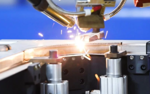
Laser Soldering leverages the energy of a laser beam to melt solder paste or pre-deposited solder, creating reliable electrical connections without physically touching the PCB. Unlike conventional soldering, which often heats a larger area, Laser Soldering concentrates energy at microscopic points, allowing for high-precision work even on ultra-fine pitch components.
Key mechanisms include:
-
Photon Energy Transfer – The laser emits photons that convert into heat upon absorption by the solder material.
-
Localized Melting – Only the targeted solder joint melts, reducing the risk of damage to adjacent circuits.
-
Rapid Cooling – Laser Soldering promotes fast solidification, resulting in strong metallurgical bonds and minimal residual stress.
This precision makes Laser Soldering particularly suitable for high-density PCBs, where interconnections may be narrower than 0.2 mm and any thermal overshoot could compromise board integrity.
Advantages of Laser Soldering for High-Density PCBs
Laser Soldering provides multiple advantages over traditional soldering methods:
-
Enhanced Precision and Accuracy – Micrometer-level control reduces the risk of solder bridges and defective joints.
-
Minimal Thermal Stress – Focused heat application preserves component integrity and board materials.
-
Reduced Material Waste – Only necessary solder is melted, improving efficiency.
-
Compatibility with Advanced Materials – Laser Soldering is effective for complex PCBs with exotic substrates or sensitive components.
These benefits directly contribute to improved PCB performance, higher yields, and lower failure rates. Manufacturers like SQ PCB leverage this technology to produce boards that meet rigorous quality standards for aerospace, medical, and consumer electronics.
Laser Soldering vs. Traditional Soldering Methods
The shift toward Laser Soldering in high-density PCBs is largely driven by the limitations of traditional soldering techniques. While conventional methods like wave soldering, selective soldering, and reflow soldering have served the electronics industry for decades, they face increasing challenges in modern, high-density designs.
1. Precision and Component Density
Traditional soldering often exposes multiple components to heat simultaneously. This can lead to solder bridges, uneven joints, and potential component damage, especially on boards with fine-pitch components. Laser Soldering, by contrast, delivers energy precisely to the target point, enabling soldering of ultra-fine pitch ICs and BGA components without affecting nearby elements.
2. Thermal Management
High-density PCBs are sensitive to thermal stress. Conventional soldering methods rely on bulk heating, which can warp boards, degrade substrate materials, or affect component longevity. Laser Soldering minimizes thermal exposure, applying heat only where necessary and reducing the risk of board deformation or delamination.
3. Process Efficiency
Although initial setup costs for Laser Soldering equipment can be higher, the process reduces material waste, rework, and defect rates. By contrast, traditional soldering may require multiple passes, manual corrections, or extensive inspection, increasing production time and cost.
4. Suitability for Complex Materials
Advanced high-density PCBs often use exotic materials, such as Rogers laminates or flexible substrates. These materials can be sensitive to prolonged heat exposure. Laser Soldering is compatible with such materials, ensuring reliable solder joints without damaging the substrate or nearby components.
In essence, Laser Soldering represents a paradigm shift: it addresses precision, thermal control, efficiency, and material compatibility—all critical factors for high-density PCB manufacturing. Companies like SQ PCB have adopted Laser Soldering to deliver consistently high-quality boards for cutting-edge applications.
Laser Soldering and Its Impact on PCB Reliability
Reliability is a key metric in PCB performance, particularly in high-density boards used in aerospace, medical devices, and high-frequency electronics. Laser Soldering significantly enhances reliability through several mechanisms:
-
Stronger Metallurgical Bonds – Rapid heating and cooling create dense, uniform solder microstructures, improving mechanical and electrical performance.
-
Minimized Defects – Precision soldering reduces the occurrence of solder bridges, voids, and cold joints.
-
Improved Thermal Cycling Performance – Reduced thermal stress translates to better endurance under repeated heating and cooling cycles.
-
Enhanced Signal Integrity – By maintaining precise soldering and avoiding thermal damage, Laser Soldering preserves the electrical properties of high-speed traces and critical vias.
The reliability improvements offered by Laser Soldering make it indispensable in applications where PCB failure is not an option. This has been a driving factor for the 92% adoption rate in high-density PCB production.
Case Studies: High-Density PCB Success with Laser-Soldering
The practical advantages of Laser Soldering become evident when examining real-world applications. High-density PCBs used in consumer electronics, aerospace, and medical devices demonstrate the technique’s transformative impact.
Case Study 1: Smartphone Motherboards
Smartphone motherboards are among the densest PCBs in production today. Manufacturers face challenges such as ultra-fine pitch ICs, high I/O counts, and sensitive substrates. By adopting Laser Soldering, manufacturers were able to:
-
Achieve micrometer-level precision in component placement.
-
Reduce solder bridge defects by over 70%.
-
Improve board reliability under thermal cycling tests.
This not only enhanced product durability but also reduced rework costs, making Laser Soldering a cost-effective solution despite higher initial investment.
Case Study 2: Aerospace Electronics
Aerospace applications demand the highest reliability standards. PCBs must withstand extreme temperatures, vibration, and prolonged service life. Laser Soldering provided:
-
Localized heating that minimized thermal stress on critical components.
-
Stronger metallurgical bonds, improving mechanical integrity.
-
Consistent solder quality for high-frequency signal traces.
The adoption of Laser Soldering allowed aerospace manufacturers to meet stringent reliability requirements while maintaining tight production schedules.
Case Study 3: Medical Devices
High-density PCBs in medical devices, such as diagnostic equipment and implantable electronics, require flawless operation. Laser Soldering enabled:
-
Precise soldering of miniature components.
-
Reduced risk of component failure due to thermal exposure.
-
Increased yield rates in production, ensuring timely device delivery.
These examples clearly illustrate why Laser Soldering has become the standard for high-density PCB assembly. For manufacturers seeking a reliable partner in implementing this technology, SQ PCB offers advanced solutions tailored to high-density and high-reliability applications.
SQ PCB: Your Partner for Advanced Laser-Soldering Solutions
SQ PCB has emerged as a leader in high-density PCB manufacturing, particularly in implementing Laser Soldering. Their expertise ensures that manufacturers can fully leverage the benefits of this technology without compromising quality or efficiency.
Key offerings include:
-
Precision Laser Soldering Services – Micrometer-level control to solder ultra-fine pitch components.
-
High-Reliability PCB Production – Rigorous quality control ensures consistent solder integrity and mechanical performance.
-
Support for Complex Materials – SQ PCB handles advanced substrates, including Rogers laminates and flexible PCBs.
-
Customized Solutions – Tailored processes to meet specific application requirements in aerospace, medical, and consumer electronics.
By partnering with SQ PCB, companies can accelerate adoption of Laser Soldering while minimizing risk, maximizing yield, and maintaining competitive advantage.
Common Challenges and Solutions in Laser-Soldering
While Laser Soldering offers significant advantages for high-density PCBs, it is not without challenges. Understanding these limitations and implementing effective solutions ensures optimal performance and reliability.
1. High Initial Equipment Cost
Laser Soldering systems require significant capital investment, which can be a barrier for smaller manufacturers.
Solution: Focus on long-term ROI. The reduced defect rates, minimized rework, and higher yields often offset the initial expenditure within a short production cycle. Partnering with specialized providers like SQ PCB can also reduce setup complexity and cost.
2. Precision Alignment Requirements
Laser Soldering demands extremely accurate alignment between the laser and the target pad. Misalignment can cause incomplete solder joints or component damage.
Solution: Implement automated vision-guided systems and calibration routines to ensure micrometer-level precision.
3. Heat-Sensitive Components
Even localized heat from a laser can affect highly sensitive components if improperly applied.
Solution: Optimize laser power, pulse duration, and focal length based on component type and solder material. Simulation and testing are critical before large-scale production.
4. Solder Paste Compatibility
Not all solder pastes respond equally to laser energy. Some pastes may require different melting profiles to achieve proper wetting.
Solution: Use solder pastes specifically designed for laser applications and perform pre-production trials to confirm compatibility.
5. Operator Training
Laser Soldering requires skilled technicians capable of managing equipment and process parameters.
Solution: Provide comprehensive training programs and ongoing process monitoring to maintain high-quality standards.
By addressing these challenges systematically, manufacturers can fully exploit Laser Soldering advantages, ensuring consistent solder quality, reduced defects, and superior PCB performance.
Future Trends of Laser-Soldering in PCB Manufacturing
The adoption of Laser Soldering is expected to grow further as high-density PCB designs become more complex. Key trends shaping the future include:
1. Integration with Automated Manufacturing
Combining Laser Soldering with automated pick-and-place and inspection systems will further increase production speed and accuracy.
2. Advanced Materials
Emerging PCB substrates, including ultra-thin and flexible boards, will increasingly rely on Laser Soldering for reliable component attachment.
3. Miniaturization of Components
As ICs continue to shrink, Laser Soldering will become indispensable for soldering micro-BGA packages, chip-scale packages (CSPs), and other ultra-fine components.
4. AI and Machine Learning
AI-assisted laser systems can optimize soldering parameters in real time, reducing defects and improving throughput.
5. Environmental Considerations
Laser Soldering is inherently cleaner than traditional wave soldering, reducing flux and lead contamination and supporting green manufacturing initiatives.
The trajectory of these trends indicates that Laser Soldering will remain a cornerstone of high-density PCB manufacturing, driving both innovation and efficiency across industries.
Conclusion: Why Laser-Soldering is Essential for Modern Electronics
The rapid advancement of high-density PCB designs has transformed the electronics industry, demanding unprecedented levels of precision, reliability, and efficiency. Traditional soldering methods, while historically effective, increasingly fall short in addressing the challenges posed by ultra-fine components, complex substrates, and high-performance requirements.
Laser Soldering has emerged as the definitive solution, offering:
-
Micrometer-Level Precision – Ensuring solder joints are accurate even in densely packed boards.
-
Minimal Thermal Stress – Protecting both components and substrates from heat-induced damage.
-
Enhanced Reliability – Producing stronger metallurgical bonds and reducing defects such as voids, cold joints, and solder bridges.
-
Material Versatility – Compatible with advanced, flexible, and high-performance PCB substrates.
Case studies from consumer electronics, aerospace, and medical devices demonstrate that Laser Soldering not only improves production yields but also ensures long-term performance under demanding conditions. Companies like SQ PCB have embraced this technology to deliver boards that meet the highest standards of quality and reliability.
As PCB technology continues to evolve—with miniaturization, flexible electronics, and high-frequency designs becoming more common—Laser Soldering will remain a critical enabler of innovation. Its ability to precisely join components without compromising board integrity ensures that manufacturers can meet growing performance demands while reducing production risk.
In conclusion, the adoption of Laser Soldering in over 92% of high-density PCBs is no accident. It represents a strategic response to the complex challenges of modern electronics manufacturing, securing both the performance and reliability that today’s advanced applications require.
FAQs About High-Density PCBs and Laser-Soldering
1. What is the difference between rolled copper foil and electrolytic copper foil?
Rolled copper foil is produced by mechanically rolling copper into thin sheets, offering better surface quality and mechanical strength. Electrolytic copper foil is deposited via an electrolytic process and is more flexible and cost-effective. The choice between the two affects PCB performance, particularly in high-frequency or high-density applications.
2. How does Laser-Soldering improve solder joint reliability compared to traditional methods?
Laser Soldering provides precise, localized heating, minimizing thermal stress on the PCB and components. This results in stronger metallurgical bonds, fewer solder defects such as voids or bridges, and improved performance under thermal cycling.
3. Can Laser-Soldering be used on flexible PCBs?
Yes, Laser Soldering is highly suitable for flexible and exotic PCB materials. Its localized heat application prevents warping or damage to sensitive substrates, making it ideal for high-density flexible circuit designs.
4. What are the main limitations of Laser-Soldering?
The primary challenges include high initial equipment cost, precision alignment requirements, sensitivity of components to heat, solder paste compatibility, and the need for trained operators. These limitations can be mitigated with proper planning, automation, and partner support, such as services provided by SQ PCB.
5. Why is Laser-Soldering increasingly preferred in high-density PCBs?
As component density increases and feature sizes shrink, traditional soldering methods struggle with precision and reliability. Laser Soldering addresses these challenges, offering superior accuracy, minimal thermal stress, higher yields, and compatibility with advanced materials. This explains its adoption in over 92% of high-density PCB production.

- long board pcb
- Flexible PCBs
- Special PCB
- Express Printed Circuit Board
- Pcb Prototype
- LED PCB
- PCB
- Printed Circuit Board
- Pcb meaning
- Pcb manufacturer
- Rigid pcb board
- Rigid Flex PCB
 Quote
Quote
 E-mail