Introduction
In the intricate world of printed circuit boards (PCBs), many elements contribute to the flawless functioning of modern electronic devices. Among these, one crucial yet often overlooked component is the Earthing Layer — the silent guardian that ensures stability, reliability, and safety. Though not always visible or discussed, earthing layers play an indispensable role in protecting PCBs from electrical noise, interference, and potential damage.
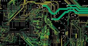
Earthing layers
1. Understanding Earthing-Layers: A Detailed Introduction
What Are Earthing Layers?
Earthing layers, sometimes referred to as ground planes or ground layers, are dedicated conductive layers within a PCB designed primarily to establish a low-resistance path to the earth or ground reference point. Their fundamental purpose is to stabilize voltage levels, provide a return path for electrical currents, and shield the circuit from unwanted electromagnetic interference (EMI).
Typically composed of copper, these layers are strategically embedded within multilayer PCBs or placed on inner layers for complex designs. The copper used may vary in thickness and type depending on the application, but their core function remains constant: creating a consistent and effective grounding scheme that enhances the circuit’s electrical integrity.
Composition and Structure
Earthing layers are generally large copper areas spread across one or more layers inside the PCB stack-up. Unlike signal traces, which are thin and narrow, earthing layers form broad, continuous conductive surfaces that can cover most of the PCB’s inner layers.
The thickness of copper used in these layers varies, commonly ranging from 1 oz (35 µm) to 3 oz (105 µm) per square foot, depending on the thermal and electrical requirements. Thicker copper provides better conductivity and heat dissipation but increases manufacturing cost.
Placement of Earthing-Layers in PCBs
In multilayer PCB designs, earthing layers are often placed as inner layers sandwiched between signal layers. This strategic placement offers several advantages:
-
Electromagnetic Shielding: The earthing layer acts as a shield to prevent noise from coupling into signal layers.
-
Signal Integrity: It provides a stable reference plane for signals, minimizing signal distortion and crosstalk.
-
Thermal Management: The copper mass helps dissipate heat generated by components and traces.
In simpler two-layer PCBs, earthing is typically managed by dedicated ground traces or copper pours on the bottom layer.
Variations by PCB Type
-
Rigid PCBs: Usually have one or more dedicated earthing layers inside the multilayer stack-up.
-
Flexible PCBs: Earthing layers may be thinner or use flexible copper foils but maintain similar functionality.
-
Rigid-Flex PCBs: Combine both types with tailored earthing layers adapted for flexibility and rigid sections.
2. Earthing-Layers and Their Importance in PCB Performance
Electrical Noise Reduction and EMI Shielding
One of the primary reasons earthing layers are crucial is their role in minimizing electromagnetic interference (EMI). Electronic components and high-speed signals inherently generate EMI, which can disrupt nearby circuits and degrade performance.
Earthing layers serve as a low-impedance path to ground for these stray currents and noise. By providing a broad, continuous conductive surface, earthing layers absorb and redirect interference, effectively shielding sensitive signal layers.
Enhancing Signal Integrity
Signal integrity refers to the accuracy and quality of the electrical signals traveling through a PCB. Earthing layers support signal integrity by acting as a reference plane for return currents. A solid ground plane reduces impedance discontinuities and limits the loop area formed by signal-return paths, decreasing signal reflections and crosstalk.
This effect is especially significant in high-speed digital and RF circuits, where signal degradation can severely impact device function.
Thermal Management Benefits
Apart from electrical performance, earthing layers help in thermal dissipation. Copper’s excellent thermal conductivity enables earthing layers to spread heat generated by components, preventing hot spots and improving overall reliability.
Overall Reliability and Lifespan
By maintaining a stable ground reference and reducing electrical noise, earthing layers help extend the operational lifespan of PCBs. They reduce stress on components caused by voltage fluctuations and transient voltages, lowering failure rates.
3. Design Considerations for Effective Earthing-Layers in PCBs
Optimizing Earthing-Layers in Multilayer PCB Design
Designing an effective earthing layer requires thoughtful integration into the PCB stack-up. Typically, placing the earthing layer adjacent to one or more signal layers helps ensure a solid reference plane and minimal electromagnetic interference. In multilayer PCBs, designers often allocate one or two inner layers exclusively for earthing to maximize shielding.
A well-implemented earthing layer reduces loop areas of high-frequency signals, thus improving signal integrity. The key is to maintain continuous copper without unnecessary splits or cuts, as discontinuities can increase impedance and create unwanted noise.
Layer Stack-Up Strategies Involving Earthing Layers
A common stack-up strategy involves sandwiching signal layers between ground (earthing) and power planes. This “stripline” configuration offers excellent noise immunity and reduces electromagnetic emissions.
Alternatively, a “microstrip” design places the signal layer adjacent to a ground plane but on the PCB surface, suitable for simpler or cost-sensitive applications.
Choosing the right stack-up depends on electrical requirements, cost constraints, and mechanical considerations.
Impact of Copper Thickness and Foil Types on Earthing Layers
Copper thickness significantly influences the performance of earthing layers. Thicker copper offers lower resistance and better heat dissipation but increases manufacturing costs and board weight.
Regarding copper foil types, the choice between rolled copper foil and electrolytic copper foil can affect the earthing layer’s mechanical strength and surface properties. Rolled copper foil, with its smoother surface and superior mechanical properties, is ideal for high-reliability applications, whereas electrolytic copper foil offers cost benefits with more flexibility.
Importance of Via Stitching and Grounding Strategies
Via stitching connects earthing layers vertically through the PCB, enhancing the low-impedance path to ground and reducing EMI. Strategically placed stitching vias improve shielding effectiveness and thermal conduction.
Grounding strategies should aim for a single-point or multipoint ground system depending on frequency and circuit design, avoiding ground loops which can induce noise.
Design Trade-Offs: Cost, Performance, and Manufacturability
While thick, continuous earthing layers improve performance, they raise manufacturing complexity and costs. Designers must balance electrical benefits with budget and production capabilities.
Collaborating with experienced PCB manufacturers, such as SQ PCB, can help optimize these trade-offs by leveraging their design expertise and advanced fabrication technologies.
4. Manufacturing Challenges and Quality Control of Earthing-Layers
Common Defects Related to Earthing Layers
During manufacturing, several defects can compromise earthing layers, including:
-
Delamination: Separation between layers causing loss of conductivity.
-
Poor adhesion: Weak bonding of copper foil to substrate reducing reliability.
-
Voids or air pockets: Interruptions in the copper layer leading to high resistance.
-
Over-etching: Excessive copper removal thinning the earthing layer.
Such defects can degrade the earthing layer’s effectiveness and lead to premature PCB failure.
Inspection Techniques for Earthing-Layer Integrity
To ensure earthing layers meet quality standards, manufacturers use various inspection methods:
-
Automated Optical Inspection (AOI): Detects surface defects and pattern inconsistencies.
-
X-ray Imaging: Reveals internal layer defects and voids.
-
Electrical Testing: Measures continuity and resistance of earthing layers.
-
Cross-Section Analysis: Physically examines layer adhesion and thickness.
Role of PCB Manufacturers Like SQ PCB in Ensuring High-Quality Earthing-Layers
Top-tier PCB fabricators, including SQ PCB, invest heavily in process control and quality assurance to deliver reliable earthing layers. They employ advanced lamination techniques, precision etching, and rigorous testing protocols to minimize defects.
By partnering with experienced manufacturers, designers can be confident that the earthing layers in their PCBs will meet performance and durability expectations.
Process Improvements for Better Earthing Layer Performance
Continuous advancements in material science and fabrication technology allow for improved earthing layers. These include enhanced copper foils with better conductivity, surface treatments improving adhesion, and cleaner lamination environments reducing contamination.
Manufacturers also adopt stricter process controls and real-time monitoring to catch defects early, ensuring consistent quality.
5. Future Trends in Earthing-Layers for Next-Generation PCBs
Emerging Materials and Technologies Improving Earthing-Layers
The future of earthing layers lies in innovative materials and fabrication methods. Researchers are exploring advanced copper alloys, graphene-infused layers, and novel conductive polymers to enhance conductivity, flexibility, and thermal management.
Additionally, nanotechnology is enabling ultra-thin but highly efficient earthing layers suitable for compact and flexible electronics.
Integration with Advanced PCB Technologies
As PCBs evolve, earthing layers must adapt to technologies such as High-Density Interconnect (HDI), flexible PCBs, and RF/microwave boards. These applications demand more precise control over grounding and shielding.
For instance, flexible PCBs require earthing layers that maintain integrity under bending, while RF boards rely on carefully engineered ground planes for signal fidelity.
Environmental and Sustainability Considerations
Sustainable manufacturing is gaining importance. New processes aim to reduce copper waste and energy consumption during lamination. Recycling methods for PCB materials are also improving, encouraging manufacturers like SQ PCB to adopt greener practices.
How Companies Like SQ PCB Are Adapting
SQ PCB leads by integrating these trends into their production lines, offering advanced earthing layer solutions that meet the demands of modern electronics while emphasizing quality and sustainability.
Conclusion
Earthing-layers may be hidden within the complex stack-up of a PCB, but their role as a protective shield is undeniable. They safeguard circuits from noise, enhance signal quality, assist thermal management, and ultimately increase the reliability and lifespan of electronic devices.
For designers and manufacturers, understanding and prioritizing the implementation of effective earthing layers is essential. Partnering with reputable PCB fabricators like SQ PCB ensures that these critical layers meet the highest standards of quality and performance.
As electronics continue to advance, the importance of well-designed earthing layers will only grow, cementing their position as the silent yet vital backbone of every reliable PCB.
FAQs About Earthing Layers in PCBs
Q1: What is the difference between rolled copper foil and electrolytic copper foil?
Rolled copper foil is produced by mechanically rolling copper into thin sheets, offering better surface quality and mechanical strength. Electrolytic copper foil is deposited via an electrolytic process and is more flexible and cost-effective.
Q2: How do Earthing Layers reduce electromagnetic interference?
Earthing layers provide a continuous conductive path to ground, which absorbs and redirects electromagnetic noise, preventing it from coupling into sensitive signal lines.
Q3: Can Earthing Layers affect thermal dissipation in PCBs?
Yes, the copper in earthing layers conducts heat away from components, helping to spread and dissipate heat, thereby improving thermal management.
Q4: What are common mistakes in designing Earthing Layers?
Mistakes include having split or incomplete ground planes, insufficient via stitching, and placing earthing layers too far from signal layers, all of which can increase noise and reduce effectiveness.
Q5: How do manufacturing processes influence the quality of Earthing Layers?
Processes like lamination pressure, temperature control, and cleanliness impact copper adhesion and layer integrity. Poor control can lead to defects such as delamination and voids that degrade performance.

- long board pcb
- Flexible PCBs
- Special PCB
- Express Printed Circuit Board
- Pcb Prototype
- LED PCB
- PCB
- Printed Circuit Board
- Pcb meaning
- Pcb manufacturer
- Rigid pcb board
- Rigid Flex PCB
 Quote
Quote
 E-mail