1. Introduction to Broken Circuit: Understanding PCB Reliability Challenges
In modern electronics manufacturing, the reliability of printed circuit boards (PCBs) is foundational. Among the various failure modes, Broken Circuit stands out as one of the most insidious and challenging to detect and prevent. Unlike visible defects, broken circuits can be microscopic cracks, subtle layer delaminations, or tiny plating voids that interrupt electrical continuity. These faults may manifest as intermittent failures, making troubleshooting difficult and time-consuming.
Broken Circuit failures occur when the conductive path — whether a copper trace, via, or pad — is physically interrupted. This results in an open circuit where electrical signals cannot propagate, leading to partial or total device failure. The challenge is compounded by the fact that broken circuits often arise during or after manufacturing, frequently induced by mechanical stresses, thermal cycling, or environmental exposure during device usage.
As electronic devices become smaller and more complex, with finer trace geometries and multi-layer constructions, the likelihood of broken circuit defects increases if not properly managed. This necessitates a comprehensive understanding of broken circuits, their causes, and effective prevention methods.
This article will serve as a detailed guide for engineers, designers, and manufacturers facing the toughest PCB reliability challenges related to broken circuits. We will explore technical details, share practical recommendations, and provide real-world examples to help you minimize these failures in your products.
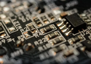
Broken Circuit
2. Common Causes of Broken Circuit in PCB Manufacturing (Expanded)
To effectively address broken circuits, it is crucial to understand their root causes during PCB manufacturing and lifecycle:
2.1 Mechanical Stress and Handling
Handling of PCBs during assembly is one of the most common causes of broken circuits. During processes such as depaneling, insertion, soldering, or even transportation, mechanical forces like bending, twisting, or dropping can cause copper traces or vias to crack.
In particular, rigid-flex PCBs and thinner rigid boards are more susceptible to such damage. Sharp bends or flexing beyond the design limits can lead to delamination between layers and micro-fractures in copper conductors. Even when the damage is not immediately visible, such micro-cracks can propagate over time and cause intermittent or permanent broken circuits.
2.2 Incomplete Copper Plating and Etching Defects
The copper plating process is essential in creating robust conductive paths, especially for plated through-holes (vias). Defects like insufficient plating thickness or uneven deposition can create weak spots prone to fracture.
Etching defects such as over-etching can thin traces excessively or cause undercutting, weakening the trace mechanically. Conversely, under-etching may leave residual copper, leading to shorts. Both defects can contribute to broken circuit failures.
2.3 Thermal Cycling and Environmental Stress
Electronic products often undergo repeated heating and cooling cycles during operation, repair, or environmental changes. This thermal cycling causes materials in the PCB to expand and contract.
When different materials — such as copper foil, laminate substrate, and solder mask — have mismatched coefficients of thermal expansion (CTE), internal stresses build up. Over time, this stress leads to cracks in copper traces or separation between layers (delamination), resulting in broken circuits.
2.4 Poor Material Quality
Using low-grade or incompatible PCB materials is a common contributor to broken circuit problems. Low Tg (glass transition temperature) laminates can soften under heat, increasing the risk of delamination and trace cracking.
Similarly, poor quality copper foils lacking tensile strength or proper adhesion layers can break under stress. Adhesive layers that degrade over time under heat or humidity allow layers to separate.
2.5 Design Flaws
Improper design practices also increase the risk of broken circuits. This includes:
-
Trace widths that are too narrow to withstand mechanical and thermal stress.
-
Sharp 90-degree corners which concentrate electrical and mechanical stress.
-
Insufficient via plating thickness or poorly designed via structures.
-
Lack of mechanical reinforcement in high-stress regions.
Good design for manufacturability (DFM) guidelines must be followed to avoid these risks.
3. Broken Circuit Impact: Why Reliability Matters in PCBs (Expanded)
When a broken circuit occurs, the resulting failure can have a domino effect on the entire system or device.
3.1 Commercial Impact
Failing PCBs lead to costly product recalls, repairs, or replacements. Companies face significant warranty expenses and potential legal liabilities, especially in industries like medical devices and aerospace.
3.2 Customer Trust and Brand Reputation
Repeated failures due to broken circuits undermine confidence in a brand, leading to loss of customers and reduced market share.
3.3 Production Delays and Increased Costs
Defective PCBs cause rework and slow down production lines, increasing labor and overhead costs.
3.4 Safety and Compliance Risks
In critical applications such as automotive or healthcare, broken circuit failures can cause hazardous situations or non-compliance with industry regulations.
4. Broken-Circuit Prevention Strategies in Design and Fabrication
Effective prevention of broken circuits starts early, with design considerations and process controls:
4.1 Design for Manufacturability (DFM)
-
Use trace widths and spacing that meet or exceed IPC standards.
-
Avoid sharp angles in traces that can concentrate stress.
-
Ensure sufficient via plating and consider redundant vias for critical nets.
-
Incorporate mechanical reinforcements if the PCB will endure bending.
4.2 Material Choices
Selecting materials with compatible coefficients of thermal expansion (CTE) reduces thermal stress.
High-quality copper foils and laminates enhance adhesion and reduce cracking risks.
4.3 Process Control and Inspection
-
Maintain tight control over plating and etching parameters.
-
Use in-line optical inspection and electrical testing to catch defects early.
-
Implement automated optical inspection (AOI) and flying probe tests.
4.4 Handling and Assembly
-
Train personnel on careful PCB handling to prevent mechanical damage.
-
Use protective packaging and minimize bending during assembly.
5. Material Selection and Its Role in Broken-Circuit Prevention
The choice of materials has a direct impact on the robustness of the PCB against broken circuits:
-
Copper Foil: Rolled copper foil offers superior mechanical strength compared to electrolytic foil. While electrolytic foil is more flexible and cost-effective, rolled copper’s higher tensile strength makes it less prone to cracking.
-
Laminates: High Tg (glass transition temperature) laminates improve resistance to thermal cycling.
-
Adhesives: High-quality adhesives maintain layer integrity and reduce delamination risks.
Selecting the right materials early on not only prevents broken circuits but also enhances overall PCB reliability.
6. Advanced Testing Techniques for Detecting Broken-Circuit Issues
Detecting broken circuits before assembly is crucial. Common methods include:
-
Electrical Continuity Testing: Verifies that all intended electrical paths are complete.
-
Automated Optical Inspection (AOI): Detects physical defects such as cracks or missing copper.
-
X-Ray Inspection: Identifies internal faults like via voids or hidden cracks.
-
Thermal Imaging: Locates hot spots indicating high resistance or intermittent breaks.
Using a combination of these testing methods ensures early detection and reduction of faulty PCBs reaching the assembly line.
7. Environmental Factors Contributing to Broken-Circuit Failures
Environmental stresses can exacerbate broken circuit issues, such as:
-
Humidity and Moisture: Can cause corrosion or delamination.
-
Vibration and Shock: Lead to mechanical stress and crack formation.
-
Temperature Extremes: Accelerate material fatigue and expansion/contraction cycles.
Designing PCBs with environmental conditions in mind and choosing suitable protective coatings can help mitigate these risks.
8. Case Studies: Real-World Broken-Circuit Problems and Solutions
To illustrate the challenges and solutions for broken circuits, consider these scenarios:
-
Case 1: A consumer electronics device repeatedly failed in drop tests due to thin copper traces cracking. Solution: Increased trace width and switched to rolled copper foil, improving mechanical strength.
-
Case 2: An industrial controller showed intermittent faults after thermal cycling. Solution: Selected a high Tg laminate and improved via plating thickness, eliminating the broken circuit root cause.
Such examples emphasize the importance of a comprehensive approach to prevent broken circuits.
9. The Role of Automation in Minimizing Broken-Circuit Risks
Automation in PCB manufacturing, including robotic handling, automated testing, and process control, helps reduce human error and mechanical damage, which are common causes of broken circuits. SQ PCB, for instance, utilizes state-of-the-art automated systems to ensure consistent quality and reliability, minimizing the incidence of broken circuits in their PCBs.
10. How SQ PCB Supports Reliability in Broken-Circuit Prevention
SQ PCB is a leading PCB manufacturer known for stringent quality control and material selection that help prevent broken circuits. Their expertise in using rolled copper foil and advanced laminates combined with automated inspection ensures that customers receive PCBs with minimal risk of broken-circuit failures. Choosing SQ PCB means investing in reliability that supports long-term product success.
11. Emerging Technologies Addressing Broken-Circuit Challenges
Technological advances, such as:
-
Flexible and Rigid-Flex PCBs: Designed to withstand bending without trace breakage.
-
Nano-coatings and Conformal Coatings: Enhance environmental resistance.
-
3D Printing and Additive Manufacturing: Allow precise control of trace geometries reducing defects.
These innovations are shaping the future of PCB reliability and reducing broken circuit issues.
12. Best Practices for Long-Term Reliability and Maintenance
-
Implement routine electrical and visual inspections during product life.
-
Use protective conformal coatings to guard against environmental damage.
-
Avoid mechanical stress during maintenance or repair.
-
Design for easy diagnostics to quickly isolate broken circuit failures.
Conclusion: Moving Beyond Broken-Circuit to Robust PCB Solutions
Addressing broken circuit challenges requires a multifaceted approach — from thoughtful design, quality material selection, and precise manufacturing to thorough testing and proper handling. Leveraging trusted suppliers like SQ PCB ensures you benefit from their quality standards and technology to mitigate broken circuit risks. As electronics grow more complex and demand higher reliability, proactive broken circuit prevention will be essential for sustained success.
Frequently Asked Questions about Broken-Circuit and PCB Reliability
Q1: What is the difference between rolled copper foil and electrolytic copper foil?
Rolled copper foil is produced by mechanically rolling copper into thin sheets, offering better surface quality and mechanical strength. Electrolytic copper foil is deposited via an electrolytic process and is more flexible and cost-effective.
Q2: How does thermal cycling cause broken circuits?
Thermal cycling causes expansion and contraction in materials. If the PCB layers have mismatched expansion rates, stress builds up and can crack copper traces or separate layers.
Q3: Can broken circuits be repaired on a finished PCB?
Minor broken traces can sometimes be repaired using conductive inks or solder bridges, but this is often a temporary fix and not recommended for critical applications.
Q4: How does SQ PCB ensure minimal broken circuit defects?
SQ PCB uses high-quality materials, strict process controls, and automated inspection to catch defects early, ensuring high reliability.
Q5: Are flexible PCBs less prone to broken circuits?
Flexible PCBs can better withstand bending stresses, but their design and material selection are crucial to prevent broken circuits.

- long board pcb
- Flexible PCBs
- Special PCB
- Express Printed Circuit Board
- Pcb Prototype
- LED PCB
- PCB
- Printed Circuit Board
- Pcb meaning
- Pcb manufacturer
- Rigid pcb board
- Rigid Flex PCB
 Quote
Quote
 E-mail