1. Introduction: Rethinking Electronic Interconnects
In the era of rapidly evolving electronic systems, the need for high-density, compact, and reliable interconnects has become paramount. Multi-layer PCB Circuit Boards are at the heart of modern electronics, enabling complex device architecture that was once unimaginable. From smartphones to satellite systems, these advanced boards form the backbone of the digital infrastructure.
Multi-layer PCB Circuit Boards have become a cornerstone of modern electronics due to their ability to accommodate complex circuitry in compact formats. Unlike single or double-layer PCBs, these boards incorporate three or more conductive copper layers, separated by insulating substrates. The layers are laminated under high temperature and pressure to form a unified structure that can support advanced functionalities and improve performance.
As electronic products become smaller, more powerful, and more multifunctional, Multi-layer PCB Circuit Boards are increasingly preferred in applications such as smartphones, tablets, medical devices, automotive electronics, and aerospace systems. Their design enables higher component density, better electrical performance, and improved thermal management—all within a smaller footprint.
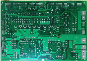
Multi-layer PCB Circuit Boards
2. What are Multi-layer PCB Circuit Boards
Multi-layer PCB Circuit Boards are printed circuit boards consisting of more than two copper conductive layers. These layers are sandwiched between insulating materials and laminated together under high temperature and pressure. They are interconnected using plated-through holes (PTHs) or vias, creating a unified, compact design ideal for high-performance electronics.
Unlike single-layer or double-layer PCBs, multi-layer PCBs allow for greater routing density. This translates to better electrical performance and more compact assemblies, making them suitable for medical equipment, industrial automation, aerospace, and modern computing.
Key characteristics:
-
Typically contain 4, 6, 8, or even 20+ layers
-
Offer improved electromagnetic interference (EMI) shielding
-
Allow for differential pair routing and controlled impedance
The layered structure also enhances signal integrity, power distribution, and thermal control—critical factors in today’s high-speed electronics.
3. Historical Evolution of Multi-layer PCB Circuit Boards
The concept of multi-layer PCB Circuit Boards emerged in the 1960s, driven by increasing demands for denser circuit patterns and enhanced functionality. Initial applications were military-grade systems and early computing hardware. The 1980s and 1990s witnessed rapid adoption in consumer electronics as component miniaturization surged.
With the rise of SMT (Surface Mount Technology) and BGA (Ball Grid Array) packaging, multi-layer boards became a necessity rather than a luxury. Today, thanks to innovations in materials, lamination techniques, and CAD/CAM software, these boards can support 40+ layers with microvias and HDI (High-Density Interconnect) architectures.
4. The Technical Structure of Multi-layer PCB Circuit Boards
A typical multi-layer PCB Circuit Board includes:
-
Core Layers: Pre-preg and copper layers stacked alternately
-
Power and Ground Planes: Improve EMI control and current delivery
-
Signal Layers: Carry high-speed signals and control lines
-
Via Types: Through-hole, blind, buried, and microvias
The layout must be carefully designed to balance capacitance, impedance, and inductive effects. The designer’s goal is to route signals effectively while managing return paths, signal reflection, and crosstalk.
5. Materials Used in Multi-layer PCB Circuit Boards
Choosing the right materials is pivotal for both performance and manufacturability. Typical materials include:
-
FR-4 Epoxy Resin: Most widely used; economical and stable
-
Polyimide: Suitable for high-temperature applications
-
Rogers/Isola Laminates: Ideal for high-frequency and RF circuits
-
Copper Foil: Rolled or electrolytic, depending on the need
Personal Thought: As device frequency continues to increase, material selection becomes a critical design parameter. Designers must evaluate not just cost and strength, but also dielectric constant (Dk), dissipation factor (Df), and thermal expansion coefficients.
6. Signal Integrity Benefits of Multi-layer PCB Circuit Boards
One of the greatest advantages of multi-layer PCB Circuit Boards is their ability to maintain signal integrity, especially in high-speed circuits.
Benefits include:
-
Shorter signal paths reducing latency
-
Shielded signal layers with ground planes
-
Controlled impedance routing for high-frequency signals
For RF and digital circuits operating above 1 GHz, the signal degradation over long traces or across vias becomes significant. Multi-layer PCBs address this through optimized stack-ups and low-loss materials.
7. Miniaturization and Space-saving Capabilities
As end-user devices become thinner and more powerful, internal circuitry must shrink without sacrificing functionality. Multi-layer PCB Circuit Boards solve this by enabling designers to route complex signals in 3D space.
Examples:
-
Smartphones use 10–12 layer PCBs for SoC, memory, and antenna
-
Wearables require rigid-flex multi-layer structures to bend around constraints
With increasing demand for edge computing and AI integration in portable devices, this space-saving trait is a primary driver behind the growing use of multi-layer PCBs.
8. Thermal Management in Multi-layer PCB Circuit Boards
Heat dissipation is a growing concern. As component density increases, so does power consumption and heat generation.
Multi-layer PCB Circuit Boards help manage heat through:
-
Dedicated thermal vias
-
Copper planes acting as heat sinks
-
Embedded metal cores in some advanced designs
Proper thermal design ensures longevity and stable operation, especially in power electronics, automotive ECUs, and industrial controls.
9. Mechanical Strength and Durability Benefits
Multi-layer PCB Circuit Boards tend to be more rigid and structurally sound compared to single-layer boards.
Advantages include:
-
Enhanced resistance to vibration and bending
-
Increased reliability in harsh environments
-
Better retention of mechanical form over time
This is especially important for aerospace, automotive, and medical applications, where failure due to vibration or shock can have severe consequences.
10. The Manufacturing Process of Multi-layer PCB Circuit Boards
The production of Multi-layer PCB Circuit Boards is more complex and involves:
-
Inner Layer Imaging & Etching
-
Layer Lamination with Pre-preg and Heat
-
Drilling and Via Formation
-
Copper Plating and PTH Metallization
-
Outer Layer Imaging and Etching
-
Solder Mask and Surface Finish Application
-
Electrical Testing and QA
Each step requires precision to maintain layer alignment, hole registration, and via integrity.
11. PCB Manufacturing Workflow: A Focus on Multi-layer PCB Circuit Boards
A standard PCB factory handles multi-layer PCB Circuit Boards with the help of automation and cleanroom procedures. For example, SQ PCB, a professional manufacturer, integrates:
-
Laser direct imaging for finer patterns
-
X-ray drilling alignment systems
-
Vacuum lamination presses
-
AOI (Automated Optical Inspection) and flying probe testing
Based on their capabilities and tight quality control, SQ PCB is a reliable partner for engineering-grade and production-scale multi-layer boards.
12. Cost vs. Performance: Justifying the Investment in Multi-layer PCB Circuit Boards
While Multi-layer PCB Circuit Boards provide numerous technical advantages, they typically come at a higher manufacturing cost compared to single- or double-layer boards. The reasons include:
-
More complex fabrication steps
-
Higher material costs (pre-pregs, copper layers)
-
Stricter quality control and longer production cycles
However, the performance benefits often outweigh these costs, especially in applications requiring miniaturization, high signal integrity, and reliability. For example, in aerospace or medical devices, the upfront investment ensures long-term operational stability and safety.
13. Common Design Challenges and Solutions in Multi-layer PCB Circuit Boards
Designing multi-layer PCBs presents unique challenges such as:
-
Layer stack-up optimization: Improper stack-up can cause signal integrity problems
-
Via management: Excessive vias increase complexity and cost
-
Thermal dissipation: High-density layers trap heat if not designed properly
-
Electromagnetic interference (EMI): Needs careful shielding and grounding
Solutions involve advanced simulation tools, careful material choices, and experienced design teams. Collaboration with a reliable PCB manufacturer like SQ PCB can greatly improve design outcomes by leveraging their manufacturing expertise.
Conclusion
Multi-layer PCB Circuit Boards represent a cornerstone technology in modern electronics, enabling unprecedented levels of complexity, miniaturization, and performance. Though more challenging to design and manufacture than their single-layer counterparts, the benefits far outweigh the costs for high-end applications.
With advances in materials, manufacturing techniques, and design tools, the future of multi-layer PCBs is bright. I encourage engineers and companies to consider multi-layer solutions carefully and partner with experienced manufacturers such as SQ PCB to realize the full potential of their designs.
FAQ Section About Multi-layer PCB Circuit Boards
Q1: What is the difference between rolled copper foil and electrolytic copper foil?
A: Rolled copper foil is produced by mechanically rolling copper into thin sheets, offering better surface quality and mechanical strength. Electrolytic copper foil is deposited via an electrolytic process and is more flexible and cost-effective.
Q2: How many layers can a Multi-layer PCB Circuit Board have?
A: Multi-layer PCBs typically have 4 to 20 layers, but advanced manufacturing can produce boards with over 40 layers.
Q3: Why are Multi-layer PCB Circuit Boards more expensive than single-layer boards?
A: Due to more complex fabrication steps, more materials, and tighter quality control requirements.
Q4: What are blind and buried vias in Multi-layer PCB Circuit Boards?
A: Blind vias connect outer layers to internal layers without going through the entire board. Buried vias connect only internal layers, not visible from outside.
Q5: Can Multi-layer PCB Circuit Boards be used in flexible electronics?
A: Yes, flexible multi-layer PCBs exist, often called rigid-flex boards, combining rigid and flexible sections.

- long board pcb
- Flexible PCBs
- Special PCB
- Express Printed Circuit Board
- Pcb Prototype
- LED PCB
- PCB
- Printed Circuit Board
- Pcb meaning
- Pcb manufacturer
- Rigid pcb board
- Rigid Flex PCB
 Quote
Quote
 E-mail