In PCB manufacturer, the choice of copper thickness must be compatible with line width and spacing to ensure manufacturability, yield, and long-term reliability. A common design mistake engineers make—especially in pursuit of high current or thermal performance—is specifying 2oz copper thickness with very fine line/space such as 6mil/6mil. But here’s the kicker: this combination can push manufacturing to its physical limits.
Let’s walk through the technical reasons why.
What Are Line Width and Line Spacing?
In PCB design, line width (trace width) is the width of the copper trace that carries electrical signals or power. Line spacing is the distance between two adjacent copper lines. These parameters are typically measured in mils (1 mil = 0.001 inches ≈ 25.4μm).
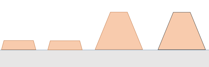
From a cross-sectional view, a trace isn’t a perfect rectangle. Instead, due to chemical etching, it takes on a trapezoidal shape—wider at the top and narrower at the bottom. The thicker the copper, the more exaggerated this slope becomes.
Line Width and Spacing Design
How to Properly Measure Line Width from the Side
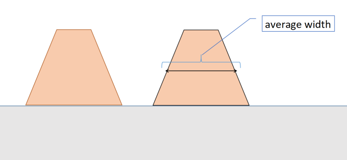
When evaluating whether your PCB meets design requirements, it’s crucial to know where to measure the trace width—especially since traces don’t have perfectly vertical walls due to the etching process.
From a side (cross-sectional) view, a copper trace usually takes on a trapezoidal shape, not a rectangle. That means:
-
The top of the trace is wider (due to mask opening)
-
The bottom of the trace is narrower (due to side etching)
📌 So where should you measure the line width?
The correct and industry-standard measurement point is at the bottom of the trace, where it meets the dielectric (base material).
This is because:
-
The bottom width determines electrical resistance, current-carrying capacity, and etching accuracy.
-
It reflects the true minimal conductor width, which affects reliability.
At SQPCB, we use cross-sectioning tools and high-magnification imaging to measure line width precisely at the correct position, ensuring that your PCB meets IPC-defined quality standards—especially for Class 2 and Class 3 boards.
line width
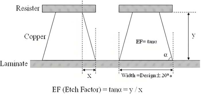
What Is the Etching Factor?
This is where things get interesting.
The Etching Factor is a key metric that describes how controllable the PCB etching process is. It’s defined as:
Etching Factor = Trace Height (Copper Thickness) ÷ Side Etch Amount
In simple terms, the higher the etching factor, the more “vertical” and clean the trace walls are. The lower the etching factor, the more the trace becomes slanted, malformed, or even etched away entirely.
Industry-standard etching factors typically range from 2:1 to 4:1. When the factor drops below 1.5:1, manufacturing becomes unstable, and quality is compromised.
Etching Factor
Why 6mil/6mil Cannot Be Paired with 2oz Copper
Now for the core issue in PCB supplier…
Let’s do the math:
-
2oz copper = approx. 70μm thickness
-
In wet etching, side etch = 60~70μm, often close to or equal to copper thickness
-
For a 6mil trace (≈150μm), subtracting side etch on both sides leaves only ~20μm of copper at the trace base
This results in:
-
Etching factor ≈ 70μm ÷ 65μm ≈ 1.08 → TOO LOW
-
Extremely thin trace roots prone to breakage, necking, or open circuits
-
Line spacing shrinks below safety limit, increasing risk of short circuits or bridging
Simply put, you may end up with no trace at all, or a weak, unreliable one.
Recommended Copper Thickness vs. Line Width Table
| Copper Thickness | Typical Side Etch | Minimum Recommended Line Width / Spacing | Etching Factor Status |
|---|---|---|---|
| 0.5oz (17μm) | 4~6μm | ≥3mil | Excellent (EF > 3.0) |
| 1oz (35μm) | 10~18μm | ≥4~6mil | Good (EF ≈ 2.0–3.0) |
| 2oz (70μm) | 30~50μm | ≥8~10mil | Risky (EF < 1.5) |
| 3oz+ | 50μm+ | ≥12mil | Extremely difficult |
So, for 6mil/6mil designs:
-
Use 0.5oz or 1oz copper thickness
-
Copper Thickness vs. Line Width
Avoid 2oz unless your line/space is ≥8mil, and you’ve discussed it with your manufacturer
A Word from the Experts: SQPCB
At SQPCB, we understand the complex trade-off between copper thickness, line resolution, and manufacturability. Our in-house engineers and process experts routinely assist clients in optimizing their designs for both performance and production yield.
Need high-current capability with tight traces?
We’ll evaluate your requirements and offer intelligent compromises—such as local thickening, dual copper weights, or optimized stack-ups.
With our LDI direct imaging, fine-line etching control, and IPC Class 3 capability, we can confidently deliver solutions that others might reject as too risky.
Conclusion
Using 6mil/6mil trace and space with 2oz copper may seem like a performance upgrade—but in reality, it introduces serious manufacturing risks. The etching factor drops, traces deform, and yield drops dramatically.
If your project demands high current or thermal performance, consider increasing trace widths, using wider spacing, or using 1oz copper with double traces instead.
Want reliable guidance? Partner with SQPCB, where engineering meets practicality, and every design is verified by seasoned pcb meaning experts.
FAQ
Q1: What happens if I insist on using 2oz copper with 6mil/6mil design?
You’ll likely encounter severe yield issues. The etching factor drops below the acceptable threshold, resulting in line thinning, potential open circuits, and shorts due to inadequate spacing and trace integrity loss.
Q2: Can LDI (Laser Direct Imaging) or advanced etching improve this situation?
LDI improves resolution and alignment but does not eliminate the physical limitations of thick copper and fine traces. Even with advanced imaging, 2oz with 6mil/6mil is still at the edge—or beyond—of most manufacturers’ process capability.
Q3: Why does thicker copper increase side etch?
The etching process removes copper both vertically and laterally. The thicker the copper, the longer the exposure time required, which increases side etching proportionally. This lateral loss of material is what reduces the bottom width of the trace.
Q4: Are there any workarounds to use 2oz copper in high-density designs?
Yes. Techniques like step-etching, split copper weights, or using localized heavy copper areas can help. However, these require early design consultation with your PCB manufacturer and additional cost considerations.
Q5: What line width and spacing are safe for 2oz copper in standard production?
Generally, 8mil/8mil or larger is the safe minimum for 2oz copper. For better yield and etch quality, many manufacturers prefer 10mil/10mil or more when dealing with 2oz or heavier copper weights.

- long board pcb
- Flexible PCBs
- Special PCB
- Express Printed Circuit Board
- Pcb Prototype
- LED PCB
- PCB
- Printed Circuit Board
- Pcb meaning
- Pcb manufacturer
- Rigid pcb board
- Rigid Flex PCB
 Quote
Quote
 E-mail