In the world of electronics, bare PCBs are the foundational element on which many devices are built. Ready for the good part? Whether you’re designing consumer electronics, automotive systems, or medical devices, understanding bare PCBs is essential. This article will explain what a bare PCB is, its manufacturing process, applications, and how it fits into the larger world of electronics. By the end, you’ll have a solid understanding of why bare PCBs are crucial in the world of modern technology.
What is a Bare PCB
1. Introduction to Bare PCBs
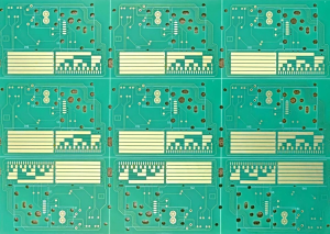
A bare PCB is an unpopulated circuit board that consists of a flat surface made from an insulating material with copper traces. These traces form the electrical connections between various components like resistors, capacitors, and microchips. But here’s the kicker? Despite being “bare,” the PCB serves as the backbone of virtually every electronic device, supporting and connecting all the essential components to ensure the device functions properly.
The term “bare” refers to the fact that the PCB has no components or solder on it. Once populated with components and connected, the bare PCB becomes the fully functional board that powers the devices we use daily. The design and quality of the bare PCB are crucial because it dictates how well the assembled device will perform.
Bare PCBs are used in many different applications, from consumer electronics like smartphones and laptops to medical devices and automotive systems. Understanding the different types of bare PCBs and how they are made is essential for any engineer or designer working in electronics.
Table 1: Basic Characteristics of a Bare PCB
| Characteristic | Description |
|---|---|
| Material | Typically made from fiberglass (FR4) or other composite materials |
| Surface | Copper traces are printed on a non-conductive surface |
| Usage | Base for attaching electronic components |
| Finish | Bare PCBs are free from solder or components |
2. Bare PCB Materials
The materials used in manufacturing bare PCBs are crucial because they affect the performance, cost, and longevity of the board. Ready for the kicker? Different materials are chosen based on the specific needs of the PCB’s intended application, whether it’s for high-frequency communication, heat dissipation, or environmental resilience.
1. FR4: The Most Common Material
The most common material used for bare PCBs is FR4, a composite of fiberglass and epoxy resin. FR4 is popular because it provides an excellent balance of durability, insulation properties, and cost-effectiveness. It’s a versatile material that can be used in most general-purpose electronics applications, such as consumer devices, computers, and industrial machines.
2. Flexible PCBs: Polyimide
For flexible PCBs, which are used in wearable devices and applications where the board needs to bend or flex, polyimide is often the material of choice. Polyimide provides high-temperature resistance, chemical stability, and flexibility, making it ideal for products like medical devices and wearables.
3. High-Frequency Materials
In applications where high-speed signals need to travel through the PCB, such as in RF (Radio Frequency) devices or high-performance communication systems, materials like PTFE (Teflon) or ceramics are used. These materials have low dielectric constants, which help in reducing signal loss and interference.
Table 2: Types of Bare-PCB Materials
| Material | Description | Applications |
|---|---|---|
| FR4 | Fiberglass and epoxy composite material | Consumer electronics, industrial systems |
| Polyimide | Flexible material for PCBs | Wearables, medical devices |
| PTFE | High-frequency material for RF applications | Communication systems, antennas |
| Ceramic | High-temperature resistant material | High-power and automotive systems |
3. How Bare-PCBs Are Manufactured
The process of creating a bare-PCB is highly detailed and involves several steps to ensure quality and functionality. Ready for the good part? Here’s a step-by-step breakdown of the bare PCB manufacturing process.
1. Designing the PCB
The first step in creating a bare PCB is designing the circuit layout. Engineers use PCB design software like Altium Designer or Eagle to create the schematic. The design includes copper traces, pads for components, and vias (small holes) for interlayer connections.
2. Printing the Design
Once the design is complete, it is printed onto a copper-clad laminate using a process called photoresist. This involves covering the PCB with a light-sensitive film and exposing it to ultraviolet (UV) light through the printed design, which then hardens the film. The unhardened sections are washed away, leaving behind a protective layer that shields the copper from the etching process.
3. Etching the Copper
The next step is etching, where the copper is exposed to a chemical solution that removes the unprotected copper, leaving behind only the copper traces that form the electrical pathways. The result is a bare PCB with all its copper traces intact.
4. Drilling and Plating
Once the copper traces are in place, holes are drilled into the PCB to accommodate vias and component leads. The PCB is then plated with nickel and gold (or other materials, depending on the finish), which makes the traces conductive and ready for component placement.
5. Final Cleaning
The last step involves cleaning the PCB thoroughly to remove any contaminants or leftover chemicals. The bare-PCB is now ready to be populated with components.
Table 3: PCB Manufacturing Process Overview
| Step | Description | Purpose |
|---|---|---|
| Design | PCB layout is created using design software | Ensures proper routing of signals |
| Printing | The design is printed onto the copper-clad laminate | Transfers the schematic onto the PCB |
| Etching | Unprotected copper is removed through chemical solution | Creates the copper traces on the PCB |
| Drilling and Plating | Holes are drilled and plated for vias and components | Prepares the PCB for component assembly |
| Cleaning | PCB is cleaned to remove contaminants | Prepares the PCB for the final use |
4. Applications of Bare-PCBs
Bare-PCBs are found in a wide variety of applications. From everyday gadgets to advanced industrial machines, their role in modern technology cannot be overstated. Ready for the kicker? Bare-PCBs are the foundation of nearly all electronic devices.
1. Consumer Electronics
Bare PCBs are used in consumer electronics such as smartphones, tablets, and computers. These devices rely on bare PCBs to connect components such as processors, memory chips, and displays. The designs are often compact, and bare PCBs with multi-layered structures are used to optimize space.
2. Automotive Applications
Bare-PCBs play a significant role in automotive electronics, including engine control units (ECUs), airbag systems, and infotainment systems. The need for high durability and heat resistance makes FR4 and other advanced materials the preferred choices for automotive PCBs.
3. Industrial and Medical Devices
In industrial machines, bare-PCBs serve as the backbone for control systems, sensors, and actuators. In the medical field, bare PCBs are used in critical devices such as pacemakers, heart monitors, and diagnostic equipment, where reliability and precision are paramount.
Table 4: Common Applications of Bare PCBs
| Industry | Application | Example Devices |
|---|---|---|
| Consumer Electronics | Smartphones, laptops, tablets | iPhone, MacBook |
| Automotive | Engine control units, safety systems | Airbag systems, engine controllers |
| Industrial | Control systems, automation, sensors | Robotics, factory machinery |
| Medical | Diagnostic equipment, life-saving devices | Pacemakers, MRI machines |
5. Bare PCBs vs. Assembled PCBs
Understanding the difference between a bare PCB and an assembled PCB is crucial when designing electronics. What’s the real story? While bare PCBs are unpopulated, assembled PCBs have components mounted on them, allowing them to perform the intended functions.
Bare PCBs
A bare PCB is simply a base that has the necessary traces for electrical connections but lacks components such as resistors, capacitors, or microchips. These boards are often used for prototyping or testing before moving on to the final product assembly.
Assembled PCBs
An assembled PCB, on the other hand, is fully populated with components that allow it to perform its intended task. These are the functional PCBs that are used in end-products, whether it’s a smartphone, medical device, or industrial equipment.
Why Choose Bare PCBs?
Bare PCBs are usually chosen for applications where the electronic components will be placed by hand or using automated machines. They’re ideal for initial testing, prototyping, and situations where a custom PCB design needs to be created.
Table 5: Bare PCB vs. Assembled PCB
| Feature | Bare PCB | Assembled PCB |
|---|---|---|
| Components | No components, just copper traces | Fully populated with electronic components |
| Application | Prototyping, custom design | Final product used in devices |
| Cost | Lower cost | Higher cost due to component assembly |
| Functionality | Requires additional assembly | Fully functional and ready to use |
6. The Vital Role of Bare PCBs in Electronics
In conclusion, bare PCBs are fundamental to the functioning of modern electronics. They provide the essential framework for connecting components and ensuring the proper operation of devices. Ready for the kicker? While they may appear simple, bare PCBs are the cornerstone of electronic innovation, from consumer gadgets to industrial machinery. Their flexibility, cost-effectiveness, and role in prototyping make them invaluable to the manufacturing and design process. As technology continues to advance, the role of bare PCBs will only grow, becoming more sophisticated and integral to the development of next-generation devices.
A3: Common materials include FR4 (fiberglass and epoxy), polyimide (for flexible PCBs), and ceramic for high-performance applications.
7. Bare PCBs in Prototyping and Testing
When developing new electronic devices, bare PCBs are often the first step. Ready for the good part? Prototyping with bare PCBs allows designers and engineers to test and iterate their designs before committing to the full assembly process. This is critical in ensuring that the final product meets the required specifications and performs as expected.
1. Why Use Bare PCBs in Prototyping?
Bare PCBs are ideal for prototyping because they offer flexibility and cost-efficiency. Engineers can quickly create custom PCB designs and test them before going into full-scale production. This helps identify potential issues early in the design process, reducing the risk of costly mistakes later on.
2. Prototyping Process with Bare-PCBs
The prototyping process typically involves the following steps:
- Designing the Circuit: The first step is to design the circuit using PCB design software like Altium Designer or Eagle.
- Printing the Bare-PCB: Once the design is complete, it is printed onto a bare-PCB, which serves as a test platform for components.
- Testing the Prototype: The bare-PCB is populated with the necessary components, and the circuit is tested for functionality, performance, and reliability.
After testing, designers can modify the design, if necessary, and create a new version of the PCB to improve performance.
3. Benefits of Using Bare-PCBs for Prototyping
Using bare-PCBs for prototyping provides numerous benefits. For one, it allows manufacturers to quickly test and iterate on new designs. It also helps save costs in the early stages of product development, as bare-PCBs are cheaper than fully assembled PCBs. Additionally, bare PCBs are highly customizable, making it easier to adjust designs and test various configurations.
Table 6: Prototyping Process with Bare PCBs
| Step | Description | Purpose |
|---|---|---|
| Circuit Design | Create the circuit design using PCB design software | Ensures functionality of the board |
| Printing the Bare-PCB | Print the design onto a copper-clad laminate | Forms the base of the prototype |
| Testing the Prototype | Populate the PCB with components and test functionality | Identify design flaws or areas of improvement |
8. The Importance of Bare -PCBs in Modern Electronics
Bare-PCBs are fundamental to the operation of modern electronics. What’s the real story? Without them, there would be no functional circuit boards connecting components, which are the heart of any electronic device. The versatility of bare PCBs makes them suitable for a wide range of applications, from consumer electronics to high-performance computing.
1. High-Density Circuit Designs
One of the driving forces behind the demand for bare-PCBs is the increasing complexity of circuit designs. Multi-layered PCBs are often used in devices where space is at a premium, such as smartphones and wearables. The flexibility of bare-PCBs allows for intricate designs that can accommodate a large number of components in a compact form.
2. Rapid Technological Advancements
The pace of technological advancement means that new devices are constantly being developed. Bare PCBs are at the core of these innovations, allowing for rapid iteration and modification in the design phase. From the prototype stage to the final assembly, bare PCBs serve as the foundation for future technology.
3. The Impact of Bare-PCBs on Miniaturization
Bare PCBs are integral to the trend of miniaturization in electronics. As devices become smaller, the need for high-density interconnect (HDI) PCBs has grown. These advanced PCBs, often made with bare-PCB material, offer more layers in less space, allowing for smaller and more powerful devices.
Table 7: Bare PCBs and Miniaturization in Electronics
| Technology | Impact on Bare-PCBs | Applications |
|---|---|---|
| High-Density Circuit | More layers in smaller form factors | Smartphones, wearables, laptops |
| Miniaturization | Smaller components, more compact boards | IoT devices, portable electronics |
| Technological Advancements | Faster design iterations and prototyping | Consumer electronics, medical devices |
9. Common Challenges with Bare-PCBs
Despite their widespread use, bare-PCBs come with their own set of challenges. But here’s the kicker? Identifying these challenges early in the design and manufacturing process can help mitigate potential issues down the road.
1. Manufacturing Defects
One of the most common issues with bare PCBs is manufacturing defects, such as etching errors or poorly placed vias. These defects can cause the PCB to fail when it is populated with components, leading to costly delays in the production process.
2. Handling and Storage
Bare PCBs are sensitive to physical damage and environmental conditions. Moisture, dust, and static electricity can all affect the PCB’s performance. It’s essential to handle and store bare PCBs properly to prevent damage or contamination during the manufacturing process.
3. Compatibility with Components
Bare PCBs are designed to connect components, but sometimes there are compatibility issues with component leads or pads. This can result in poor solder joints, leading to functionality issues in the finished product. Ensuring that the PCB design is compatible with the components being used is critical to avoid these problems.
Table 8: Common Challenges with Bare PCBs
| Issue | Description | Solution |
|---|---|---|
| Manufacturing Defects | Errors in etching, vias, or copper placement | Implement quality control checks |
| Handling and Storage | Moisture, dust, and static damage to bare PCBs | Store PCBs in controlled environments |
| Component Compatibility | Misalignment of component leads or pads | Ensure accurate design and alignment with components |
10. Bare-PCBs in High-Performance and Advanced Applications
Bare PCBs are essential in high-performance applications, where reliability and precision are key. Ready for the good part? These applications often demand advanced materials and designs that can handle high-speed signals, heat dissipation, and extreme environmental conditions.
1. High-Frequency Applications
Bare PCBs are used in high-frequency electronics, including RF circuits and 5G devices. These applications require materials that minimize signal loss and provide electrical insulation. Teflon-based and ceramic-based bare PCBs are commonly used in these high-speed, high-frequency applications.
2. Automotive and Aerospace
Bare PCBs are used in automotive and aerospace applications where safety and performance are critical. For example, in automotive electronics, bare PCBs are used in engine control units (ECUs) and airbag systems, while in aerospace, bare PCBs are used in satellite communications and radar systems.
Table 9: Bare PCBs in High-Performance Applications
| Application | Material and Design Considerations | Use Cases |
|---|---|---|
| High-Frequency Circuits | Teflon or ceramic-based bare PCBs for signal integrity | RF communications, 5G devices |
| Automotive | Heat-resistant materials for durability | ECUs, safety systems, sensors |
| Aerospace | High-temperature materials for reliability | Satellites, radar systems |
11. Conclusion: The Importance of Bare-PCBs in Electronics
In conclusion, bare-PCBs are the unsung heroes of modern electronics. They are essential in everything from consumer gadgets to aerospace systems, providing the platform for all the components that make electronic devices work. Ready for the kicker? Despite their simplicity, bare PCBs are critical to the functionality, performance, and cost-effectiveness of nearly every electronic device. Understanding how bare PCBs are made, used, and their limitations will ensure you can make the best decisions for your PCB needs, whether you’re designing for consumer electronics, industrial applications, or high-performance systems.
12. The Role of Bare-PCBs in the Internet of Things (IoT)
Bare PCBs are at the heart of many Internet of Things (IoT) devices. But here’s the kicker? IoT devices are designed to be compact, efficient, and connected, and bare PCBs play a vital role in these goals. As IoT technology continues to evolve, the demand for smaller, more powerful, and cost-effective PCBs is on the rise.
1. Compact Design for Small IoT Devices
IoT devices, such as wearables, smart home devices, and healthcare monitors, require small, high-performance PCBs to fit into their compact form factors. Bare PCBs are often the go-to solution for these designs, as they allow manufacturers to customize the layout and optimize the space for components. With the use of multi-layered bare PCBs, designers can achieve higher density while keeping the device size small.
2. Connectivity and Performance
For IoT applications, connectivity is paramount. Bare PCBs are designed to support wireless communication modules like Wi-Fi, Bluetooth, and Zigbee. These PCBs ensure that signal integrity is maintained while providing a stable connection to other devices. The RF (Radio Frequency) performance of a bare PCB is crucial for the proper functioning of these IoT devices, making the design and material choice an essential factor.
3. Energy Efficiency
In the IoT world, where devices are expected to run on low power for long periods, bare PCBs play a critical role in optimizing energy efficiency. By ensuring that the components are connected efficiently with minimal power loss, bare PCBs help extend the battery life of IoT devices, which is vital in applications such as remote sensors or wearables that require low-energy consumption.
Table 10: Bare PCBs in IoT Devices
| IoT Device | Role of Bare PCB | Key Features |
|---|---|---|
| Wearable Devices | Custom designs for small, efficient PCBs | Low power consumption, small form factor |
| Smart Home Devices | Wireless communication and connectivity | Wi-Fi, Bluetooth, Zigbee support |
| Healthcare Monitors | Power-efficient PCBs for remote monitoring | Long battery life, small footprint |
13. Environmental Impact and Sustainability of Bare-PCBs
As the world shifts toward sustainability in electronics, the environmental impact of bare-PCBs becomes a crucial consideration. But here’s the kicker? While bare PCBs themselves are not inherently harmful, the processes used to manufacture them and the materials involved can contribute to environmental challenges.
1. The Environmental Impact of PCB Manufacturing
The manufacturing of PCBs can lead to pollution and waste. The chemicals used in the etching and plating processes, such as copper etching solutions, can be harmful to the environment if not handled properly. Additionally, the production of bare PCBs requires the use of energy-intensive processes, contributing to carbon emissions. Manufacturers must ensure that they comply with environmental regulations and adopt practices to reduce their ecological footprint.
2. Eco-Friendly Materials for Bare PCBs
The good news is that there is a growing trend toward eco-friendly PCB manufacturing. For instance, manufacturers are exploring the use of biodegradable materials and environmentally friendly chemicals to reduce the harmful effects of PCB production. Some companies are also working on developing green PCBs that do not contain hazardous substances like lead or halogenated flame retardants.
3. Recycling Bare-PCBs
Recycling bare PCBs is an essential part of managing their lifecycle. However, PCB recycling can be challenging due to the complex materials used in their construction. Nevertheless, advanced recycling technologies are making it easier to reclaim valuable metals, such as gold, silver, and copper, from discarded PCBs. By investing in efficient recycling methods, the environmental impact of bare PCBs can be minimized.
Table 11: Environmental Impact of Bare PCBs
| Environmental Factor | Description | Mitigation Approach |
|---|---|---|
| PCB Manufacturing Waste | Chemicals and waste produced during the etching process | Use eco-friendly chemicals and processes |
| Energy Consumption | Energy required for PCB fabrication | Implement energy-efficient manufacturing processes |
| PCB Recycling | Challenges in recycling PCBs due to complex materials | Develop advanced recycling technologies |
14. The Future of Bare-PCBs
What’s the real story? The future of bare PCBs looks promising as new technologies and materials are being introduced to enhance their performance and sustainability. With 5G, wearables, and IoT devices continuing to grow, the demand for bare PCBs will only increase.
1. Innovations in Bare-PCB Materials
New materials are being explored to improve the performance and sustainability of bare PCBs. Flexible substrates like polyimide are becoming more common, allowing for more versatile designs. In addition, metal core PCBs (MCPCBs) are gaining popularity in applications requiring better heat dissipation, like LED lighting and power electronics.
2. Advances in PCB Design
As electronics continue to shrink, so must the PCBs. High-density interconnect (HDI) technology is evolving, enabling the creation of more compact and complex PCBs. The trend towards multi-layered and stacked PCBs will continue to grow, allowing for more functionality in smaller devices. Bare-PCBs will play a crucial role in these advancements, enabling the creation of next-generation devices.
3. Sustainable PCB Production
The shift toward sustainability will impact the PCB industry. Future bare PCBs will likely be green-certified, made with eco-friendly materials and processes that minimize environmental impact. The industry will also see the rise of circular economy models, where PCBs are designed with end-of-life recycling in mind.
Table 12: Future Trends in Bare PCB Manufacturing
| Trend | Impact on Bare PCBs | Application |
|---|---|---|
| Flexible Substrates | Enable flexible, bendable PCB designs | Wearables, medical devices |
| HDI and Multi-layer PCBs | Higher density and compact designs | Smartphones, high-performance systems |
| Sustainable Production | Eco-friendly materials and manufacturing processes | Green-certified electronics |
15. Conclusion: The Vital Role of Bare-PCBs in Electronics
In conclusion, bare-PCBs are essential to the electronic industry, acting as the foundation for nearly all modern devices. From consumer electronics to medical applications, bare-PCBs serve as the critical starting point for device functionality. Ready for the kicker? As technology advances and demands increase, the role of bare PCBs will continue to evolve. With their ability to support complex designs, energy-efficient solutions, and sustainability, bare-PCBs will remain a key player in the future of electronics.
FAQ Section
Q1: What is a bare-PCB?
A1: A bare-PCB is an unpopulated circuit board made from an insulating material, with copper traces that form the electrical connections between components.
Q2: How are bare PCBs made?
A2: Bare-PCBs are made by designing the circuit, printing the design onto a copper-clad laminate, etching the copper, drilling holes, and plating the PCB for final use.
Q3: What materials are used in bare-PCBs?
A3: Common materials include FR4 (fiberglass and epoxy), polyimide (for flexible PCBs), and ceramic for high-performance applications.
Q4: What is the difference between a bare-PCB and an assembled PCB?
A4: A bare-PCB is an unpopulated board, while an assembled PCB has components attached, making it functional for end-use.
Q5: In which industries are bare-PCBs used?
A5: Bare-PCBs are used across various industries, including consumer electronics, automotive, medical devices, and industrial applications.

- long board pcb
- Flexible PCBs
- Special PCB
- Express Printed Circuit Board
- Pcb Prototype
- LED PCB
- PCB
- Printed Circuit Board
- Pcb meaning
- Pcb manufacturer
- Rigid pcb board
- Rigid Flex PCB
 Quote
Quote
 E-mail