The scrubbing process is a critical step in printed circuit board (PCB) manufacturing, ensuring the removal of contaminants and preparation of surfaces for subsequent processes. This article delves into the various facets of the scrubbing process, including its importance, methods, equipment, and best practices.
1. Introduction to the Scrubbing Process in PCB Manufacturing
In PCB manufacturing, surface cleanliness is paramount. The scrubbing process involves cleaning the PCB surfaces to remove oxides, residues, and other contaminants that could impede the performance and reliability of the final product. This step is essential for ensuring proper adhesion of solder masks, plating, and other coatings. The printed circuit board (PCB) manufacturing process involves multiple critical steps to ensure the reliability and performance of electronic devices. Among these, surface preparation plays a pivotal role in guaranteeing proper adhesion of conductive layers, resist coatings, and final finishes. The scrubbing process, a mechanical or chemical method for cleaning and conditioning PCB surfaces, is essential for removing contaminants, oxides, and residues that could impair subsequent manufacturing stages. This guide explores the intricacies of the scrubbing process, its variations, and its impact on PCB quality.
In the intricate realm of Printed Circuit Board (PCB) manufacturing, surface preparation stands as a pivotal determinant of the final product’s quality and reliability. Among the myriad of preparatory techniques, the Scrubbing Process emerges as a fundamental procedure. This process meticulously cleans the PCB surfaces, ensuring the removal of contaminants, oxides, and residues that could potentially compromise the board’s performance. By establishing a pristine surface, the scrubbing process facilitates optimal adhesion for subsequent layers, be it solder masks, plating, or other coatings. This article delves deep into the multifaceted aspects of the scrubbing process, elucidating its significance, methodologies, equipment, best practices, and its overarching impact on PCB manufacturing.
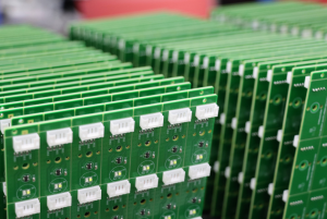
The scrubbing process
2. Importance of the Scrubbing Process in Ensuring PCB Quality
Effective scrubbing enhances the PCB’s surface quality, leading to improved electrical performance and longevity. By eliminating contaminants, the scrubbing process prevents defects such as poor solder joints and delamination, which can compromise the PCB’s functionality.
The Role of the Scrubbing Process in PCB Fabrication
Objectives of the Scrubbing Process
- Contaminant Removal: Eliminate dust, oils, and residual chemicals from previous steps (e.g., drilling, etching).
- Surface Activation: Enhance the adhesion of dry film resists, solder masks, and metal plating.
- Oxide Removal: Strip surface oxides to ensure optimal copper bonding.
Impact on Key PCB Properties
- Adhesion Strength: Poorly cleaned surfaces lead to delamination of traces or solder masks.
- Signal Integrity: Residual contaminants can cause impedance mismatches in high-frequency circuits.
- Yield Rates: Effective scrubbing reduces defects like voids in plating or solder joints.
3. Fundamental Principles Underpinning the Scrubbing Process
At its core, the Scrubbing Process is governed by principles rooted in surface chemistry and mechanical engineering. The primary objective is to achieve a contaminant-free surface that promotes optimal adhesion and electrical performance. This necessitates the removal of both organic and inorganic residues, including oxides, dust particles, and processing chemicals. The process balances mechanical action, often through brushing or abrasive techniques, with chemical action, utilizing cleaning agents tailored to dissolve specific contaminants. Critical parameters such as brush pressure, rotational speed, choice of abrasive materials, and cleaning solution composition are meticulously calibrated. These factors are adjusted based on the PCB’s material composition, design intricacies, and the nature of contaminants present, ensuring that the scrubbing process is both effective and non-damaging.
4. Mechanical Scrubbing: Equipment and Parameters
Brush Scrubbing Systems
- Horizontal vs. Vertical Scrubbers:
- Horizontal: Suitable for rigid PCBs; brushes rotate parallel to the panel.
- Vertical: Ideal for thin or flexible PCBs; brushes move perpendicularly.
- Key Parameters:
- Brush Pressure: 10–30 psi (excessive pressure can damage delicate traces).
- Brush Speed: 100–300 RPM (optimized based on contamination level).
- Abrasive Type: Carbonundum-embedded brushes for heavy scrubbing; softer brushes for post-etch cleaning.
Pumice Scrubbing Workflow
- Slurry Application: Spray or immerse PCBs in pumice-water mixture.
- Mechanical Agitation: Conveyor belts pass panels under rotating brushes.
- Rinsing: High-pressure deionized (DI) water removes abrasive residues.
Challenges in Mechanical Scrubbing
- Brush Wear: Frequent replacement required for consistent performance.
- Surface Damage: Over-scrubbing can thin copper layers or create micro-scratches.
5. Chemical Scrubbing: Formulations and Process Control
Acid-Based Scrubbing
- Sulfuric Acid Scrubbing:
- Concentration: 5–10% H₂SO₄ at 40–60°C.
- Reaction: Dissolves copper oxides (CuO → Cu²⁺ + H₂O).
- Neutralization: Sodium bicarbonate (NaHCO₃) rinse to halt acid activity.
- Hydrochloric Acid Scrubbing:
- Use Cases: Pre-plating cleaning for ENIG (Electroless Nickel Immersion Gold).
- Limitations: Aggressive on solder masks; requires precise dwell time.
Alkaline Scrubbing
- Sodium Hydroxide Solutions:
- Concentration: 2–5% NaOH at 50–70°C.
- Mechanism: Saponifies organic oils and fluxes.
- Surfactant Additives:
- Role: Reduce surface tension for better penetration into microvias.
Process Monitoring and Optimization
- pH Control: Maintain ±0.2 pH tolerance to avoid over-etching.
- Temperature Stability: ±2°C to ensure consistent reaction rates.
- Chemical Lifetime: Titration tests to monitor bath exhaustion.
Types of Scrubbing Processes in PCB Manufacturing
Mechanical Scrubbing
- Brush Scrubbing:
- Tools: Nylon or abrasive-filled brushes.
- Process: Rotating brushes physically scrub the PCB surface under controlled pressure.
- Applications: Heavy contamination removal (e.g., debris from drilling).
- Pumice Scrubbing:
- Abrasive Slurry: A mixture of pumice powder and water.
- Mechanism: Abrasive particles mechanically scour the surface.
- Advantages: Effective for removing stubborn oxides.
Chemical Scrubbing
- Acidic Cleaners:
- Agents: Sulfuric acid (H₂SO₄) or hydrochloric acid (HCl) solutions.
- Use Cases: Oxide removal from copper surfaces.
- Alkaline Cleaners:
- Agents: Sodium hydroxide (NaOH) or potassium hydroxide (KOH).
- Use Cases: Organic contaminant dissolution.
Advanced Scrubbing Techniques
- Ultrasonic Scrubbing:
- Principle: High-frequency sound waves create cavitation bubbles that dislodge contaminants.
- Advantages: Reaches microscopic crevices; ideal for complex geometries.
- Plasma Scrubbing:
- Process: Ionized gas (e.g., oxygen plasma) reacts with organic residues.
- Applications: High-precision cleaning for HDI and flex PCBs.
6. Methods Employed in the Scrubbing Process
Several techniques are utilized in the scrubbing process, each tailored to specific requirements and contamination types:
6.1 Mechanical Scrubbing Process
Mechanical scrubbing employs brushes or abrasive pads to physically remove surface contaminants. This method is effective for eliminating oxides and residues from PCB surfaces. Equipment such as brushing machines are commonly used, featuring rotating brushes that scrub the PCB as it passes through the machine. Proper control of brush pressure and selection of appropriate abrasive materials are crucial to prevent damage to delicate PCB features.
6.2 Chemical Scrubbing Process
Chemical scrubbing involves the use of solvent-based or aqueous cleaning solutions to dissolve and remove contaminants. Solvent-based cleaning utilizes organic solvents like Isopropyl Alcohol (IPA) to dissolve flux residues and other organic contaminants. Aqueous cleaning, on the other hand, uses deionized water with additives to clean water-soluble residues. Proper handling and disposal of chemicals are essential to ensure safety and environmental compliance.
6.3 Ultrasonic Scrubbing Process
Ultrasonic scrubbing employs high-frequency sound waves to create cavitation bubbles in a cleaning solution. The implosion of these bubbles generates localized high temperatures and pressures, effectively removing contaminants from intricate PCB geometries. While effective, care must be taken to prevent potential damage to sensitive components due to the intense energy released during cavitation.
7. Equipment Used in the Scrubbing Process
Various machines and tools are utilized to perform the scrubbing process efficiently:
7.1 PCB Scrubbing Machines
These machines are designed to automate the mechanical scrubbing process, featuring conveyor systems that pass PCBs through rotating brushes and rinsing stages. They offer consistent cleaning results and can handle high volumes of PCBs, making them suitable for mass production environments.
7.2 Ultrasonic Cleaning Machines
Ultrasonic cleaners submerge PCBs in a cleaning solution and apply high-frequency sound waves to dislodge contaminants. They are particularly useful for cleaning complex assemblies with hard-to-reach areas.
7.3 Manual Cleaning Tools
For low-volume production or prototype development, manual tools such as brushes and wipes may be used. While labor-intensive, manual cleaning allows for targeted removal of contaminants and is flexible for various PCB designs.
8. Best Practices in the Scrubbing Process
To achieve optimal results, the following best practices should be observed:
-
Selection of Appropriate Cleaning Method: Choose the scrubbing technique based on the type of contaminants and the PCB’s design specifications.
-
Control of Process Parameters: Regulate factors such as brush pressure, cleaning solution concentration, and ultrasonic frequency to prevent damage to the PCB.
-
Regular Maintenance of Equipment: Ensure that scrubbing machines and tools are well-maintained to provide consistent cleaning performance.
-
Environmental and Safety Considerations: Properly handle and dispose of cleaning agents, and provide adequate training to personnel to maintain a safe working environment.
9.Historical Evolution of the Scrubbing Process in PCB Manufacturing
The journey of the Scrubbing Process in PCB manufacturing mirrors the evolution of the electronics industry itself. In the nascent stages of PCB production, manual cleaning methods predominated. Technicians employed rudimentary tools and solvents to cleanse board surfaces, a labor-intensive approach fraught with inconsistencies. As electronic devices burgeoned in complexity and miniaturization became the norm, the limitations of manual cleaning became glaringly evident. This ushered in an era of mechanized scrubbing techniques, introducing specialized equipment designed to deliver uniform and efficient cleaning. The advent of automation further revolutionized the scrubbing process, integrating it seamlessly into production lines, thereby enhancing throughput and consistency. Today, the scrubbing process stands as a testament to decades of innovation, embodying a blend of precision, efficiency, and adaptability to cater to the ever-evolving demands of PCB manufacturing.
10. Detailed Examination of the Scrubbing Process Methodologies
The Scrubbing Process encompasses a spectrum of methodologies, each tailored to address specific challenges and requirements in PCB manufacturing.
10.1 Mechanical Scrubbing Process Techniques
Mechanical scrubbing employs physical means to dislodge and remove contaminants from PCB surfaces. This is typically achieved using rotating brushes or abrasive pads that make direct contact with the board. The choice of brush material—ranging from nylon to stainless steel—and the abrasiveness are selected based on the PCB substrate and the nature of residues to be removed. While mechanical scrubbing is lauded for its efficiency, especially in removing stubborn oxides, it necessitates precise control to prevent potential damage to delicate PCB features.
10.2 Chemical Scrubbing Process Techniques
Chemical scrubbing leverages specialized cleaning agents to dissolve and lift contaminants without physical abrasion. Depending on the residue type, solvents such as isopropyl alcohol (IPA) or aqueous solutions with saponifiers are employed. This method is particularly effective for removing organic residues like flux. However, it demands stringent handling protocols to ensure operator safety and environmental compliance.
10.3 Ultrasonic Scrubbing Process Techniques
Ultrasonic scrubbing utilizes high-frequency sound waves to create microscopic cavitation bubbles in a cleaning solution. The implosion of these bubbles generates localized high-energy events that effectively dislodge contaminants, even from intricate and hard-to-reach areas of the PCB. While ultrasonic cleaning offers unparalleled thoroughness, considerations regarding the potential impact on sensitive components and the choice of compatible cleaning solutions are paramount.
10.4 Hybrid Scrubbing Process Techniques
Hybrid techniques amalgamate mechanical and chemical methods to harness the advantages of both. For instance, a PCB might undergo a gentle mechanical scrub followed by a chemical rinse to ensure comprehensive cleanliness. Such combined approaches are tailored to specific manufacturing scenarios, optimizing efficiency and effectiveness.
11. Comprehensive Overview of Equipment Utilized in the Scrubbing Process
The efficacy of the Scrubbing Process is intrinsically linked to the equipment employed. Advancements in technology have ushered in a diverse array of machinery designed to cater to varying production scales and complexities.
11.1 Automated Scrubbing Machines
Automated scrubbing machines are engineered for high-volume production environments, offering consistent and repeatable cleaning results. These machines typically feature conveyor systems that transport PCBs through multiple cleaning stages, including pre-wash, scrubbing, rinsing, and drying. The integration of sensors and programmable controls allows for real-time monitoring and adjustment of parameters, ensuring optimal performance.
11.2 Manual and Semi-Automated Scrubbing Tools
For prototype development or low-volume production, manual or semi-automated tools provide flexibility. Handheld brushes, spray systems, and localized ultrasonic baths allow technicians to focus on specific areas of the PCB. While offering precision, these methods rely heavily on operator skill and are less consistent than fully automated systems.
11.3 Specialized Ultrasonic Cleaning Equipment
Ultrasonic cleaners designed for PCBs feature tanks that hold the cleaning solution and transducers that generate ultrasonic waves. Advanced models offer features like adjustable frequencies, temperature controls, and filtration systems to enhance cleaning efficacy and accommodate a range of PCB designs and contamination levels.
12. In-depth Analysis of the Scrubbing Process Workflow
The Scrubbing Process workflow within PCB manufacturing involves a sequence of carefully calibrated steps that ensure the board surfaces are properly cleaned and prepared for downstream processes such as imaging, plating, or solder mask application. Each stage in the workflow contributes to achieving a uniform, contaminant-free surface while protecting the integrity of fine copper traces and delicate substrates.
12.1 Pre-Scrubbing Preparation in the Scrubbing Process
Before scrubbing begins, PCB panels are visually inspected and sometimes tested for surface resistance to identify any high-contamination zones. Handling is performed with gloves or vacuum grippers to prevent additional contamination. If required, panels are rinsed with deionized water to remove loose particulates. The Scrubbing Process often begins only after an initial decontamination phase is confirmed.
12.2 Wetting and Lubrication Stage in the Scrubbing Process
The first operational step in the Scrubbing Process typically involves wetting the PCB panel with deionized water or a neutral surfactant. This pre-lubrication reduces friction between brushes and the PCB, thereby preventing over-polishing or micro-abrasion of fine features. This stage is crucial, particularly in boards with thin dielectric layers or ultra-fine line widths.
12.3 Mechanical Action and Abrasive Contact in the Scrubbing Process
The primary cleaning happens during this stage. Rotating brushes—either cylindrical or flat—come into contact with the PCB surface. These brushes may be made of nylon, non-woven materials, or micro-fiber filaments. The brush pressure, rotational speed, and brushing pattern (cross-hatch, spiral, or linear) are all programmed into automated systems to ensure consistency. In multi-pass systems, panels go through several rounds of brushing, each with finer or softer abrasives.
12.4 Rinsing and Debris Removal in the Scrubbing Process
After brushing, the PCB is passed through high-pressure rinse sections where deionized water jets remove dislodged particles, loosened oxides, and any residual slurry from abrasives. Effective rinsing is essential to prevent re-deposition of particulates on the surface. In this part of the Scrubbing Process, filtering systems are also used to maintain the purity of rinse water and avoid cross-contamination between panels.
12.5 Drying and Anti-Oxidation in the Scrubbing Process
The final stage involves drying the panels using heated air knives, vacuum dewatering, or infrared drying systems. Some systems may include a chemical treatment phase where anti-oxidation solutions are applied to prevent copper re-oxidation during transit to the next stage. This ensures that the benefits of the Scrubbing Process are preserved until the imaging or coating operations begin.
13. The Role of the Scrubbing Process in Multilayer PCB Fabrication
The significance of the Scrubbing Process becomes even more pronounced in multilayer PCB production. In multilayer designs, inner layer cores must be free from particulate matter and oxides to ensure proper lamination. Any residue left after oxide treatment can cause delamination or signal degradation.
13.1 Pre-Lamination Surface Preparation via Scrubbing Process
Before lamination, the scrubbing process ensures that the oxide-treated inner layers have a uniformly roughened and contaminant-free surface. This enhances resin adhesion and prevents air entrapment during lamination, which can cause voids and reliability failures.
13.2 Fine Line Reliability and Impedance Consistency
For high-speed or RF PCBs, where controlled impedance is essential, the Scrubbing Process plays a vital role. Surface contamination or uneven roughness can alter impedance characteristics. By standardizing surface conditions across all layers, scrubbing contributes to impedance uniformity and signal integrity.
13.3 Post-Lamination and Drilling Considerations
After lamination and before drilling, the scrubbing process may be used again to remove any resin smear or residual lamination debris. In this way, it acts as both a preparation and a finishing step, ensuring clean interfaces at multiple manufacturing stages.
14. Quality Control and Inspection in the Scrubbing Process
Effective execution of the Scrubbing Process must be complemented by rigorous quality control to ensure consistency, yield, and reliability.
14.1 Inline Surface Cleanliness Measurement
Advanced inline inspection systems use light scattering or surface reflectance measurement to verify cleaning effectiveness. These tools compare post-scrubbing surfaces to calibrated cleanliness standards.
14.2 Adhesion Testing Post-Scrubbing Process
Test panels are often subjected to adhesion tests where dry film resist or solder mask adhesion is measured after the scrubbing process. Weak adhesion can indicate improper cleaning or inadequate surface roughening.
14.3 Microscopy and Cross-Section Analysis
Selected samples may undergo cross-sectioning and microscopic inspection to verify that copper thickness and pattern geometries remain undistorted after the scrubbing process. SEM imaging can be used to examine micro-roughness.
15. Challenges and Troubleshooting in the Scrubbing Process
Despite automation and control, several challenges can emerge during the Scrubbing Process, necessitating diagnostic and corrective actions.
15.1 Common Defects Originating from the Scrubbing Process
-
Over-scrubbing: Causes copper thinning or erosion of fine traces.
-
Under-scrubbing: Results in poor adhesion and contamination retention.
-
Brush wear: Leads to uneven cleaning or scratched surfaces.
-
Contaminated rinse water: Causes re-deposition of particles.
15.2 Root Cause Analysis and Preventive Measures
Using SPC (Statistical Process Control), manufacturers monitor scrubbing parameters over time to detect drift. Preventive maintenance schedules are implemented to replace worn brushes, clean filters, and calibrate pressure systems.
16. Environmental and Sustainability Considerations in the Scrubbing Process
Sustainability is increasingly influencing how manufacturers approach the Scrubbing Process.
16.1 Water Conservation and Filtration
Many systems now incorporate closed-loop water systems that recycle and purify rinse water. High-efficiency filters, activated carbon beds, and reverse osmosis are used to minimize water consumption.
16.2 Abrasive Material Recycling
Some scrubbing systems use reusable abrasive belts that can be cleaned and reapplied, reducing solid waste.
16.3 Energy Efficiency and Carbon Reduction
Modern scrubbing equipment is designed with energy-efficient motors and heat recovery systems to minimize energy usage and carbon footprint.
17. Integration of the Scrubbing Process in Smart Manufacturing
As PCB factories embrace Industry 4.0, the Scrubbing Process is increasingly integrated into smart lines with real-time monitoring and adaptive control.
17.1 IoT Sensors and Data Logging
IoT-enabled sensors track brush pressure, water temperature, motor speeds, and surface cleanliness in real time. Data is logged for traceability and predictive maintenance.
17.2 AI-Driven Process Optimization
Machine learning algorithms analyze historical process data to suggest optimal scrubbing conditions based on PCB type, layer count, and copper weight.
17.3 Digital Twin Simulation for Process Planning
Some advanced manufacturers build digital twins of the scrubbing process to simulate outcomes, test new materials, and improve first-pass yield.
18. Future Developments in Scrubbing Process Technology
The Scrubbing Process continues to evolve as PCBs become more miniaturized, complex, and functionally demanding.
18.1 Nanotechnology and Coating Compatibility
New materials may demand scrubbing techniques that ensure compatibility with nano-coatings or surface treatments used in ultra-HDIs.
18.2 Adaptive Brush Design
Brushes capable of auto-adjusting their stiffness or shape based on PCB topology are being developed, allowing safer processing of uneven surfaces.
18.3 Automation and Robotics in Scrubbing
Robotic arms may replace traditional mechanical scrubbing systems, especially for flexible PCBs or components that cannot pass through conventional machines.
19. Conclusion: The Strategic Importance of the Scrubbing Process in PCB Manufacturing
The Scrubbing Process is far more than a cleaning step—it is a strategic enabler of quality, performance, and consistency in modern PCB fabrication. Whether preparing inner layers for lamination, outer layers for imaging, or substrates for solder mask, the role of surface scrubbing is foundational.
It ensures adhesion, supports impedance control, prevents delamination, and enhances reliability across all applications—from consumer electronics to aerospace-grade circuitry. As PCB designs become denser and performance demands rise, the importance of a controlled, sustainable, and technologically advanced scrubbing process cannot be overstated.
By investing in state-of-the-art scrubbing systems, integrating them into smart manufacturing environments, and applying rigorous process controls, manufacturers safeguard their product integrity while driving down costs and waste.
In the era of 5G, AI, and IoT, where every micron matters, mastering the Scrubbing Process is a competitive imperative in the global PCB manufacturing landscape.
The scrubbing process, though often overlooked, is a linchpin in PCB manufacturing, directly influencing product reliability, performance, and yield. As the industry advances toward miniaturized, high-frequency, and flexible designs, innovations in scrubbing—from AI-driven automation to eco-friendly chemistries—will be essential. By mastering this foundational step, manufacturers can ensure their PCBs meet the escalating demands of 5G, IoT, and automotive applications, solidifying their position in the competitive electronics market.

- long board pcb
- Flexible PCBs
- Special PCB
- Express Printed Circuit Board
- Pcb Prototype
- LED PCB
- PCB
- Printed Circuit Board
- Pcb meaning
- Pcb manufacturer
- Rigid pcb board
- Rigid Flex PCB
 Quote
Quote
 E-mail