Introduction to Laser Drilling
In the modern electronics industry, Laser drilling has become an essential technology in PCB (Printed Circuit Board) manufacturing. With the increasing demand for miniaturized, high-performance, and high-density interconnect (HDI) PCBs, traditional mechanical drilling methods are reaching their limitations. Laser drilling offers a high-precision, efficient, and scalable solution for creating microvias, blind vias, and through-holes, which are critical for multi-layer PCBs.
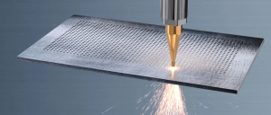
Laser drilling
The introduction of Laser drilling has transformed PCB fabrication by enabling smaller via sizes, higher interconnect densities, and enhanced electrical performance. As the industry shifts towards 5G technology, advanced computing, and IoT devices, Laser drilling plays a crucial role in achieving better signal integrity, reduced power loss, and compact circuit designs.
This article will explore:
-
The working principles of Laser drilling
-
Different types of Laser drilling techniques
-
Advantages of Laser drilling over mechanical drilling
-
Applications of Laser drilling in PCB production
-
Challenges and solutions in Laser drilling
-
Future trends in Laser drilling technology
As the demand for high-performance, miniaturized, and multi-layered PCBs (Printed Circuit Boards) continues to grow, advanced manufacturing techniques are essential to meet the increasing complexity of circuit designs. Among these techniques, Laser drilling has emerged as a critical innovation in the PCB industry. This non-contact, high-precision drilling method enables the creation of smaller, more precise via holes compared to traditional mechanical drilling methods.
Why is Laser Drilling Important for PCB Manufacturing?
The evolution of consumer electronics, 5G communication, automotive electronics, medical devices, and aerospace technology has driven PCB designs toward higher-density interconnects (HDI), finer line spacing, and smaller via sizes. Conventional mechanical drilling, which relies on rotary drill bits, faces significant limitations, such as:
-
Inability to drill extremely small microvias (below 100μm in diameter)
-
High tool wear, leading to inconsistent hole quality over time
-
Mechanical stress and delamination risks in fragile PCB substrates
Laser drilling, on the other hand, eliminates these challenges by utilizing high-energy laser beams to ablate the material precisely. This technology offers better precision, higher drilling speeds, and increased process reliability, making it indispensable in modern PCB fabrication.
The Evolution of PCB Drilling Techniques
Historically, PCB manufacturers relied on mechanical drilling for all hole formation needs. This method, while effective for larger holes and lower-density PCBs, struggled with miniaturization and multi-layer designs. As technology advanced, the demand for smaller vias, such as microvias and blind vias, increased significantly—particularly with the rise of HDI PCB technology.
With the advent of Laser drilling in the 1990s, PCB manufacturers gained a powerful tool that allowed for:
-
Drilling microvias down to 20μm, which is impossible with mechanical drilling
-
Processing rigid and flexible PCBs with minimal material stress
-
Eliminating tool wear and the need for frequent drill bit replacements
-
Enhancing production speeds, leading to cost-efficient mass production
How Laser Drilling Works
Laser drilling operates on the principle of material ablation, where a focused laser beam rapidly heats and removes material from the PCB surface. Depending on the laser type and pulse duration, different drilling effects can be achieved. The process can be broken down into the following key steps:
-
Laser Energy Absorption – The PCB material absorbs high-intensity laser light, leading to rapid heating.
-
Material Ablation or Vaporization – The concentrated heat causes the material to vaporize or melt, forming a clean hole.
-
Expulsion of Molten Material – A combination of gas pressure and laser pulses ensures smooth hole formation.
-
Cooling and Solidification – The newly formed hole cools rapidly, leaving behind a precise via with minimal burrs.
Types of Laser Drilling Techniques
PCB manufacturers employ different Laser drilling techniques depending on the required hole size, material composition, and production speed. The three most common methods include:
-
Single-Pulse Laser Drilling – A single, high-energy laser pulse is used to remove material in one step. Suitable for thin PCBs and small microvias.
-
Percussion Laser Drilling – Multiple laser pulses are applied to the same location, gradually removing material and ensuring higher hole precision.
-
Trepan Laser Drilling – The laser beam moves in a controlled circular motion, widening the hole diameter progressively. Used for larger-diameter holes.
Materials Compatible with Laser Drilling
Laser drilling is highly effective for a wide range of PCB materials, including:
-
FR-4 (Fiberglass-Reinforced Epoxy) – A common PCB substrate that requires CO₂ or UV lasers for drilling.
-
Polyimide (PI) Films – Used in flexible PCBs; UV lasers are preferred for high precision.
-
Copper Layers – Direct laser drilling on copper is challenging, but hybrid UV-CO₂ laser systems can efficiently drill through copper and dielectric layers.
-
Ceramic PCBs (Aluminum Oxide, Aluminum Nitride) – Require high-power pulsed lasers for effective drilling.
Advantages of Laser Drilling Over Mechanical Drilling
The introduction of Laser drilling in PCB manufacturing has brought numerous technical and economic advantages, making it a preferred choice over traditional mechanical drilling. Some of the key benefits include:
-
Higher Precision – Laser drilling can create smaller microvias with tighter tolerances, which is essential for HDI and multi-layer PCBs.
-
No Mechanical Wear – Since the laser is a non-contact process, there is no tool wear or degradation over time.
-
Faster Processing Speeds – Lasers can drill thousands of vias per second, making them ideal for high-volume PCB production.
-
Reduced Substrate Stress – Unlike mechanical drilling, which induces stress and delamination, laser drilling minimizes thermal and mechanical impact on the PCB.
-
Enhanced Design Flexibility – Enables more complex via structures, such as staggered vias, stacked vias, and buried vias in advanced PCB designs.
Industries Benefiting from Laser Drilling in PCBs
The adoption of Laser drilling technology has significantly impacted multiple high-tech industries, enabling next-generation electronic devices.
-
Smartphones and Consumer Electronics
-
The need for thin, lightweight, and high-performance circuit boards in smartphones, tablets, and wearables has driven Laser drilling adoption.
-
-
5G and High-Frequency PCBs
-
Millimeter-wave (mmWave) technology in 5G infrastructure requires high-precision microvias, which are best achieved through Laser drilling.
-
-
Automotive Electronics
-
ADAS (Advanced Driver Assistance Systems), electric vehicles (EVs), and in-car communication systems rely on high-density interconnect PCBs, benefiting from Laser drilling.
-
-
Medical Electronics and Wearable Devices
-
Miniaturized implantable medical devices and diagnostic equipment require extremely small vias, making Laser drilling indispensable.
-
-
Aerospace and Defense Electronics
-
Military and satellite-grade PCBs demand high-reliability via structures, which are precisely fabricated using Laser drilling.
-
Fundamentals of Laser Drilling
What is Laser Drilling?
Laser drilling is a non-contact drilling method that uses high-energy laser beams to create precise holes in PCB substrates. It relies on focused laser pulses that generate intense localized heat, causing the material to either vaporize or melt away, forming clean and precise holes.
The primary mechanisms of Laser drilling include:
-
Material Ablation – The laser removes material layer by layer, ensuring precise hole formation.
-
Thermal Decomposition – The intense heat breaks down organic substrates, creating a clean hole with minimal debris.
Compared to traditional mechanical drilling, which uses rotary drill bits, Laser drilling eliminates tool wear, mechanical stress, and size limitations, making it ideal for high-density PCB designs.
Types of Laser Drilling Methods
1. CO₂ Laser Drilling
CO₂ lasers are widely used in PCB fabrication for through-hole drilling and large via formation. They operate at wavelengths of 9.3 µm – 10.6 µm, which are well-suited for organic PCB substrates like FR-4.
Advantages of CO₂ Laser Drilling
-
High-speed processing for large-scale PCB manufacturing
-
Excellent for removing dielectric materials
-
Cost-effective for high-volume production
Limitations
-
Not suitable for drilling metallic layers
-
Limited to non-conductive PCB materials
2. UV Laser Drilling
UV lasers (ultraviolet lasers) are highly effective for microvia drilling in HDI PCBs. Operating at wavelengths around 355 nm, they offer superior precision and material selectivity.
Advantages of UV Laser Drilling
-
Creates small, high-precision microvias
-
Can drill copper, FR-4, and polyimide substrates
-
Reduces thermal damage compared to CO₂ lasers
Limitations
-
Slower processing speed than CO₂ lasers
-
Higher equipment costs
Comparison: Laser Drilling vs. Mechanical Drilling
| Feature | Laser Drilling | Mechanical Drilling |
|---|---|---|
| Precision | Extremely high (down to 20µm) | Limited by drill bit size |
| Tool Wear | No tool wear | Drill bits wear over time |
| Via Size | Can create microvias as small as 20µm | Limited to ~100µm |
| Processing Speed | Faster for microvias | Slower for fine-pitch designs |
| Heat Generation | Localized heating | Can cause substrate damage |
Applications of Laser Drilling in PCB Manufacturing
-
High-Density Interconnect (HDI) PCBs
-
Laser drilling enables fine-pitch microvias, which are crucial for HDI circuit boards used in mobile devices and wearables.
-
-
5G and RF Circuit Boards
-
Millimeter-wave frequencies require precise via structures that Laser drilling can provide.
-
-
Automotive Electronics
-
ADAS (Advanced Driver Assistance Systems) rely on Laser drilling for high-reliability PCB interconnects.
-
-
Medical Devices
-
Miniaturized implantable electronics benefit from Laser drilling in creating tiny, precise interconnections.
-
Challenges and Solutions in Laser Drilling
1. Heat-Induced Damage
-
Solution: Use short-pulse UV lasers to minimize thermal effects.
2. Copper Layer Drilling Difficulties
-
Solution: Hybrid UV-CO₂ laser drilling systems optimize metal-to-dielectric drilling.
3. Maintaining Drilling Precision
-
Solution: Implement closed-loop laser control systems for real-time adjustments.
The integration of Laser drilling in PCB manufacturing has revolutionized the electronics industry by providing unparalleled precision, efficiency, and scalability. With ongoing advancements in laser technology, we can expect even smaller vias, higher processing speeds, and improved material compatibility in the future.
As the demand for high-density, high-performance PCBs continues to rise, Laser drilling will remain a key enabler of next-generation electronic innovations.
Future Trends in Laser Drilling for PCB Production
-
Next-Generation Ultrafast Lasers
-
Femtosecond and picosecond lasers will further reduce thermal impact while improving drilling speed.
-
-
AI-Driven Laser Drilling Optimization
-
Machine learning algorithms will enhance drilling efficiency and real-time process adjustments.
-
-
Integration with 3D PCB Manufacturing
-
Additive manufacturing combined with Laser drilling will enable complex multi-layer designs.
-
Conclusion: The Future of Laser Drilling in PCB Manufacturing
The Growing Role of Laser Drilling in the PCB Industry
As electronic devices continue to become smaller, more powerful, and more complex, PCB manufacturers must keep up with the demand for precision and efficiency. Traditional mechanical drilling techniques have served the industry well for decades, but they now face significant limitations in terms of size constraints, production speed, and cost-effectiveness. The adoption of laser drilling has transformed PCB manufacturing, making it possible to create high-density interconnect (HDI) PCBs, multi-layer PCBs, and advanced electronic circuits that were previously impossible with mechanical methods.
With continued miniaturization in consumer electronics, automotive systems, aerospace technology, and medical devices, the need for high-precision laser-drilled vias will only grow stronger. As a result, laser drilling is now a critical component of PCB fabrication, allowing manufacturers to keep up with the evolving demands of the electronics industry.
Advantages That Secure Laser Drilling’s Future
The shift from mechanical drilling to laser drilling is not just a passing trend—it is a necessity driven by the many advantages laser drilling provides. These benefits ensure that laser drilling will continue to be a dominant technology in PCB manufacturing. Some of the key advantages that secure its long-term relevance include:
-
Precision at a Microscopic Scale
-
Laser drilling enables the creation of extremely small vias, with diameters as low as 20μm.
-
This precision is essential for miniaturized PCBs used in 5G devices, medical implants, and high-frequency RF circuits.
-
-
Non-Contact Process with Minimal Wear
-
Unlike mechanical drills, which suffer from tool wear over time, lasers do not degrade with usage.
-
This leads to consistent hole quality throughout production, reducing defects and improving reliability.
-
-
Higher Production Efficiency and Speed
-
Thousands of microvias can be drilled in seconds, allowing for high-volume production.
-
This efficiency is critical for mass manufacturing in industries such as automotive, telecommunications, and consumer electronics.
-
-
Versatility Across Different PCB Materials
-
Laser drilling is effective on FR-4, polyimide, ceramic, metal-core PCBs, and high-frequency laminates.
-
Multilayer stack-ups can be drilled with minimal heat damage, preserving signal integrity and material integrity.
-
-
Support for Advanced PCB Designs
-
As PCBs become more complex, staggered vias, stacked vias, and buried vias become more common.
-
Laser drilling allows for these intricate via structures to be manufactured with high accuracy.
-
Challenges That Must Be Addressed
Despite its numerous advantages, laser drilling still faces some challenges that manufacturers must overcome to fully optimize the process. Addressing these issues will ensure greater efficiency, lower costs, and wider adoption of laser drilling in PCB fabrication.
1. Heat-Affected Zones (HAZ) and Carbonization
-
Problem: Excess heat from the laser can cause carbonization or material degradation, especially in organic substrates like FR-4.
-
Solution:
-
Use shorter pulse durations (picosecond or femtosecond lasers) to minimize heat buildup.
-
Optimize laser power settings to balance efficiency with material protection.
-
2. Difficulty Drilling Through Copper Layers
-
Problem: Copper is highly reflective, making it difficult for lasers to efficiently drill through copper layers in multilayer PCBs.
-
Solution:
-
Use UV or hybrid laser systems that combine CO₂ and UV lasers to penetrate copper effectively.
-
Pre-treat copper layers with coatings that enhance laser absorption.
-
3. Cost Considerations for Small Manufacturers
-
Problem: Laser drilling systems require high initial investments, making it challenging for small-scale PCB manufacturers to adopt.
-
Solution:
-
Shared manufacturing facilities or contract services can make laser drilling more accessible.
-
As technology advances, laser system costs are expected to decrease, making them more affordable.
-
Emerging Innovations in Laser Drilling
As laser drilling technology evolves, new innovations are making it even more precise, efficient, and cost-effective. Some of the most promising advancements include:
1. Ultrafast Lasers (Picosecond and Femtosecond Lasers)
-
These next-generation lasers use extremely short pulses, reducing heat damage and enabling cleaner, more precise drilling.
-
They are particularly useful for drilling high-frequency PCBs and ceramic substrates.
2. AI and Machine Learning Optimization
-
AI-driven process monitoring helps adjust laser parameters in real-time, improving drilling accuracy and reducing defects.
-
Machine learning algorithms can optimize hole alignment, power settings, and drilling speed.
3. Hybrid Laser Systems
-
Combining CO₂, UV, and fiber lasers allows for better control over different PCB materials, including metal-core PCBs and composite substrates.
-
These systems make multilayer via drilling more efficient.
4. Automated Laser Drilling Systems
-
Fully automated drilling setups integrate robotic precision and AI-driven inspection, reducing human error and improving manufacturing yields.
Industries Driving the Growth of Laser Drilling in PCBs
1. 5G and Telecommunications
-
The rollout of 5G networks requires PCBs with high-density interconnects and precise microvias.
-
Laser drilling is essential for signal integrity in high-frequency applications.
2. Automotive Electronics
-
Electric vehicles (EVs) and autonomous driving systems require compact, high-performance PCBs.
-
Laser drilling allows for high-reliability circuits that can withstand harsh environmental conditions.
3. Aerospace and Defense
-
Military and satellite communication systems require rugged PCBs with strict tolerances.
-
Laser-drilled vias ensure reliable signal transmission in extreme environments.
4. Medical Devices
-
Implantable electronics and wearable health monitors require miniaturized PCBs with precise vias.
-
Laser drilling ensures high-precision microvias for biomedical applications.
The Road Ahead: Laser Drilling as the Standard in PCB Manufacturing
The transition from mechanical drilling to laser drilling is now inevitable. As the demand for smaller, denser, and more advanced PCB designs continues to rise, laser drilling will become the industry standard.
In the coming years, further improvements in laser precision, cost-efficiency, and automation will drive mass adoption across all major electronics sectors. Innovations in ultrafast lasers, AI-driven process optimization, and hybrid laser technologies will ensure that laser drilling remains the best solution for high-performance PCB fabrication.
Manufacturers that embrace laser drilling technology today will be well-positioned to lead the future of PCB manufacturing, ensuring higher production efficiency, better quality control, and improved product reliability.

- long board pcb
- Flexible PCBs
- Special PCB
- Express Printed Circuit Board
- Pcb Prototype
- LED PCB
- PCB
- Printed Circuit Board
- Pcb meaning
- Pcb manufacturer
- Rigid pcb board
- Rigid Flex PCB
 Quote
Quote
 E-mail