1. Introduction to Circuit Board Drill Technology
Circuit board drilling is a foundational process in PCB manufacturing, creating precise holes for vias, component leads, and mechanical mounting. As electronics shrink and complexity grows, circuit board drill technology has evolved from mechanical drilling to advanced laser systems. This guide explores the methodologies, challenges, and innovations in circuit board drill operations, offering actionable insights for engineers and manufacturers striving for precision and efficiency.
Drilling is a critical process in the manufacturing of printed circuit boards (PCBs), enabling electrical connections between different layers and facilitating the mounting of components. The precision and quality of these drilled holes significantly influence the performance and reliability of the final electronic product. This comprehensive guide delves into the intricacies of PCB drilling, exploring techniques, equipment, challenges, and advancements in the field.
In PCB fabrication, drilling involves creating holes, known as vias, that serve various purposes:
-
Through-Hole Vias: These holes traverse the entire board, connecting all layers and accommodating leaded components.
-
Blind Vias: Connecting an outer layer to one or more inner layers without penetrating the entire board.
-
Buried Vias: Located entirely within the internal layers, these vias are invisible from the outer surfaces.
The accuracy of these drilled holes is paramount, as misalignment or defects can lead to circuit failures.
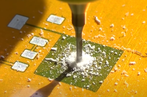
Circuit board drilling
2. Drilling Techniques in PCB Fabrication
2.1 Mechanical Drilling
Mechanical drilling employs drill bits, typically made from tungsten carbide due to its hardness and durability. This method is suitable for larger holes but faces challenges when dealing with high-density interconnects (HDI) requiring microvias.
Key Considerations:
-
Drill Bit Wear: The abrasive nature of PCB materials necessitates frequent tool replacement to maintain precision.
-
Heat Generation: High-speed drilling can cause heat buildup, potentially damaging the PCB substrate.
2.2 Laser Drilling
Laser drilling utilizes focused laser beams to ablate material, enabling the creation of microvias with diameters as small as 10 micrometers. This technique is essential for HDI PCBs, where space constraints demand smaller vias.
Advantages:
-
Precision: Allows for exact control over hole size and position.
-
Non-Contact Process: Reduces mechanical stress on the PCB.
Challenges:
-
Surface Finish: Laser-drilled vias may have inferior surface finishes, requiring additional processing.
-
Equipment Cost: High initial investment compared to mechanical drilling.
3. Drill Bit Materials and Designs
The choice of drill bit material and design directly impacts the quality and efficiency of the drilling process.
3.1 Tungsten Carbide Drill Bits
Widely used in PCB drilling, tungsten carbide bits offer high hardness and wear resistance, essential for drilling through abrasive PCB materials.
Considerations:
-
Brittleness: Requires careful handling to prevent breakage.
-
High-Speed Compatibility: Suitable for drilling at speeds up to 100,000 RPM.
3.2 Diamond-Coated Drill Bits
For specialized applications, diamond-coated bits provide enhanced durability and precision, especially in drilling hard substrates.
Benefits:
-
Extended Tool Life: Reduced frequency of bit replacement.
-
Improved Hole Quality: Minimized burring and delamination.
4. Drilling Parameters and Their Impact
Optimizing drilling parameters is crucial to achieving high-quality holes and prolonging tool life.
4.1 Spindle Speed and Feed Rate
Balancing spindle speed (RPM) and feed rate (inches per minute) is vital:
-
High Spindle Speed: Reduces cutting forces but increases heat generation.
-
Appropriate Feed Rate: Prevents excessive tool wear and ensures clean hole walls.
4.2 Peck Drilling
This technique involves retracting the drill bit periodically to remove debris, reducing heat buildup and preventing bit breakage.
5. Challenges in PCB Drilling
Several challenges can arise during the drilling process:
5.1 Smearing
High temperatures during drilling can cause resin smearing on hole walls, hindering electrical connectivity. De-smear processes, such as plasma etching, are employed to address this issue.
5.2 Drill Bit Breakage
Factors like improper feed rates, excessive spindle speeds, or worn-out bits can lead to breakage, affecting production efficiency and hole quality.
5.3 Registration Errors
Misalignment between drilled holes and PCB layers can occur due to mechanical inaccuracies, leading to defective boards.
6. Advances in PCB Drilling Technology
The PCB industry continually seeks innovations to enhance drilling precision and efficiency.
6.1 Automated Drilling Machines
Modern CNC drilling machines offer high-speed, automated drilling with minimal human intervention, improving consistency and throughput.
6.2 UV Laser Drilling
Utilizing ultraviolet lasers allows for cleaner ablation of material, resulting in superior hole quality and reduced need for post-processing.
7. Quality Control in PCB Drilling
Ensuring the integrity of drilled holes is essential for PCB functionality.
7.1 Inspection Techniques
-
Automated Optical Inspection (AOI): Detects defects such as misaligned or incomplete holes.
-
X-Ray Inspection: Identifies internal defects, including voids or misregistrations.
7.2 Testing
-
Electrical Testing: Verifies continuity and isolation of drilled vias.
-
Micro-Sectioning: Examines cross-sections of drilled holes to assess quality.
8. Compliance with Environmental Regulations
As PCB manufacturing grows, environmental concerns regarding waste disposal and emissions become more critical. Manufacturers must comply with RoHS (Restriction of Hazardous Substances) and REACH (Registration, Evaluation, Authorisation, and Restriction of Chemicals) regulations to ensure that hazardous materials from drilling processes, such as fiberglass dust and resin particles, do not contaminate the environment.
Safety Measures in PCB Drilling
To protect workers from potential hazards, manufacturers should implement strict safety protocols:
- Protective Gear: Operators should wear masks and gloves to prevent inhalation of dust and direct skin contact with harmful materials.
- Ventilation Systems: Proper air extraction systems should be in place to remove airborne particles generated during drilling.
- Automated Handling: Using robotic and automated drilling machines reduces human exposure to potential risks.
9. Cost Considerations in PCB Drilling
Optimizing the drilling process helps in cost reduction while maintaining high-quality standards.
9.1 Drill Bit Cost and Longevity
The cost of drill bits varies depending on material type, coating, and usage frequency. Tungsten carbide bits are standard due to their balance of cost and durability, but for high-precision drilling, diamond-coated bits may be used despite their higher cost.
9.2 Production Speed vs. Quality Trade-Off
Manufacturers must balance speed and quality to meet cost efficiency. Faster drilling increases throughput but may compromise hole integrity. Implementing proper feed rates and speeds can help maintain the right balance.
9.3 Yield Improvement Strategies
- Regular Maintenance of Equipment: Preventive maintenance minimizes unexpected downtime.
- Process Automation: CNC drilling machines improve consistency and reduce human errors.
- Quality Inspections: Catching defects early reduces material waste and rework costs.
10. Future Trends in PCB Drilling
With increasing demand for miniaturized and high-performance PCBs, advancements in drilling technology are inevitable.
10.1 AI-Driven Process Optimization
AI and machine learning are being integrated into PCB drilling machines to optimize drilling parameters in real time, reducing defects and improving efficiency.
10.2 Ultra-Fast Laser Drilling
New developments in ultra-fast pulsed lasers allow for more precise microvia drilling while minimizing thermal damage, making them ideal for next-generation HDI and multilayer PCBs.
10.3 Sustainable Drilling Practices
Manufacturers are shifting towards eco-friendly drilling solutions, including:
- Using water-based lubrication to reduce chemical use.
- Recycling fiberglass dust from drilling processes.
- Adopting energy-efficient drilling equipment to lower power consumption.
11. Circuit Board Drill Cost Optimization
Tooling Costs
- Drill Bit Lifecycle: Balance re-sharpening costs vs. new bit purchases.
- Laser vs. Mechanical Drill: ROI analysis for high-mix vs. high-volume production.
Energy Efficiency
- Variable Frequency Drives (VFD): Reduce spindle motor energy use by 30%.
- Laser Pulse Optimization: Minimize power consumption per hole.
12. Case Studies: Circuit board drilling in Action
Case 1: 5G mmWave Antenna PCB
- Challenge: 0.1mm microvias in PTFE substrate.
- Solution: UV laser drilling with 5µm precision, achieving 99.9% yield.
Case 2: Automotive ECU Board
- Challenge: Burr-free holes in aluminum-core PCB.
- Solution: Diamond-coated bits with peck drilling cycle, reducing deburring time by 50%.
Case 3: Medical Implantable Device
- Challenge: Drilling 0.05mm holes in ceramic-filled laminate.
- Solution: Femtosecond laser drilling eliminated micro-cracks.
13. Future Trends in Circuit board drilling Technology
Nanosecond vs. Femtosecond Lasers
- Femtosecond Lasers: Ultra-short pulses for zero heat-affected zones (HAZ).
Additive Circuit Board Drill Techniques
- 3D-Printed Vias: Conductive ink deposition in non-drilled boards.
Sustainable Circuit Board Drill Practices
- Biodegradable Coolants: Reduce environmental impact.
- Energy Recovery Systems: Capture and reuse spindle motor heat.
Conclusion: Mastering Circuit Board Drill for Next-Gen PCBs
As the demand for high-performance and miniaturized PCBs continues to rise, the role of advanced drilling technologies becomes increasingly critical. The transition from traditional mechanical drilling to laser and AI-assisted drilling marks a significant step forward in enhancing precision, efficiency, and sustainability in PCB manufacturing.
The Importance of Precision in PCB Drilling
High-density interconnect (HDI) designs, multilayer PCBs, and fine-pitch components necessitate exceptional drilling accuracy. Even minor defects, such as misaligned vias, burrs, or contamination, can lead to signal integrity issues and product failures. As a result, manufacturers must prioritize state-of-the-art drilling techniques, such as CO₂ and UV laser drilling, to ensure clean, precise hole formation with minimal material stress.
The Role of Automation and AI in Future Circuit board drilling
AI-driven drilling machines are revolutionizing PCB fabrication by dynamically adjusting drill speed, pressure, and depth in real time. This technology not only improves consistency but also reduces waste, enhances yield rates, and lowers production costs. As AI continues to evolve, we can expect:
- Real-time defect detection and correction during the drilling process.
- Self-optimizing drilling systems that adapt to different PCB materials and thicknesses.
- Predictive maintenance to prevent equipment failures and downtime.
Sustainability in Circuit board drilling
Environmental concerns are pushing PCB manufacturers to adopt greener drilling practices. Initiatives such as:
- Reducing hazardous dust emissions through advanced air filtration systems.
- Utilizing water-based lubricants instead of harmful chemical coolants.
- Recycling fiberglass and other PCB waste materials post-drilling.
help create a more sustainable and eco-friendly production environment.
Meeting Future Industry Demands
With 5G, IoT, AI, and automotive electronics driving innovation, PCB drilling must keep pace with:
- Higher layer counts and smaller vias for increased circuit density.
- More stringent reliability standards, especially for automotive and aerospace applications.
- Integration of smart manufacturing to streamline PCB fabrication.
Circuit board drilling technology sits at the heart of PCB innovation, enabling the high-density interconnects demanded by 5G, IoT, and AI hardware. By embracing advanced lasers, AI-driven optimization, and sustainable practices, manufacturers can achieve unprecedented precision while reducing costs.
Circuit board drilling remains a critical yet evolving process in circuit board manufacturing. Advances in precision drilling techniques, AI-driven optimizations, and sustainable practices are shaping the future of the industry. As demand for high-density and ultra-thin PCBs increases, manufacturers must continually adapt to new technologies to ensure high-quality, cost-effective, and environmentally responsible PCB production.
By embracing automated drilling solutions, high-precision laser technology, and AI-powered process control, PCB manufacturers can achieve higher yields, reduced defect rates, and improved overall product performance in the competitive electronics market.

- long board pcb
- Flexible PCBs
- Special PCB
- Express Printed Circuit Board
- Pcb Prototype
- LED PCB
- PCB
- Printed Circuit Board
- Pcb meaning
- Pcb manufacturer
- Rigid pcb board
- Rigid Flex PCB
 Quote
Quote
 E-mail