What Are Plated Vias?
1.Plated vias, also known as PTH (Plated Through Hole) vias, are critical structures in printed circuit boards (PCBs) used to connect electrical signals between different layers. Normally divided into through holes 3, blind holes 1, and buried holes 2 as the follow picture

Plated Vias
2. NPTH (Non-Plated Through Hole) vias are typically used for mechanical fixation or alignment and do not provide electrical connectivity.
3. Plated vias achieve electrical connections by plating a conductive material (usually copper) on the inner walls of drilled holes in the PCB. They are not only used for signal transmission but also aid in heat dissipation and enhance the mechanical strength of the PCB.
As electronic devices trend toward miniaturization, high density, and high performance, the design and manufacturing of plated vias have become increasingly important. They are an indispensable part of modern multilayer PCB designs and are widely used in consumer electronics, automotive electronics, industrial control, and communication equipment.
The Critical Role of Plated Vias in PCB Performance
Plated vias play a crucial role in the performance of circuit boards. They ensure reliable electrical connections, support mechanical stability, and contribute to thermal management. However, in reality, most customers lack specialized knowledge about circuit boards and the appropriate testing equipment to verify critical quality parameters like via copper thickness. This often leads to overlooked quality issues, which can have severe consequences in the final product.
Due to intense price competition among PCB manufacturers, many are under pressure to cut costs. Unfortunately, some manufacturers compromise on quality by reducing the copper thickness in plated vias. This cost-cutting measure can lead to significant quality problems, many of which only become apparent when the product reaches the end customer.
At sqpcb, with 14 years of experience in PCB manufacturing, we have always prioritized quality and adhered to strict standards to ensure that our customers receive reliable and high-performance products. We understand the importance of maintaining quality benchmarks, especially in critical areas like plated vias, to avoid costly failures and ensure customer satisfaction.
Types of Plated Vias
Based on their purpose and structure, plated vias can be divided into the following categories:
| Type | Description | Application |
|---|---|---|
| Through-Hole Vias | Run through the entire PCB, connecting top and bottom layers | Common in multilayer PCBs, also used for through-hole component mounting |
| Blind Vias | Connect an outer layer to an inner layer, without going through the whole board | HDI designs, space-saving |
| Buried Vias | Located entirely within the PCB, connecting inner layers only | Complex multilayer boards |
| Microvias | Diameter <150μm, made by laser drilling | High-frequency, HDI, and high-performance designs |
Functions of Plated Vias
Plated vias serve multiple functions in PCBs:
| Function | Role | Importance |
|---|---|---|
| Electrical Connectivity | Provide signal transfer between layers | Ensures circuit stability |
| Heat Dissipation | Transfer heat from components to heat sinks or other layers | Improves reliability |
| Mechanical Support | Reinforce multilayer structures | Enhances vibration resistance |
| Signal Integrity | Reduce signal loss and reflection | Critical for high-frequency circuits |
Manufacturing Process of Plated Vias
The manufacturing of plated vias is a complex process involving multiple steps and precise techniques. Here are the key steps:
1. Drilling
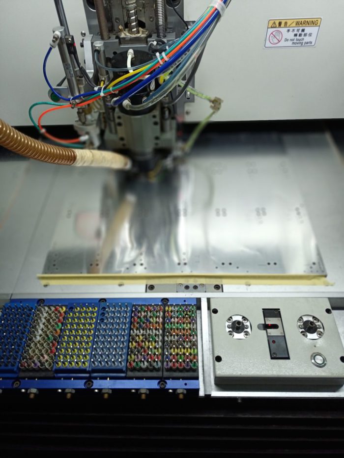
First, holes are drilled into the PCB using mechanical or laser drilling techniques. The accuracy and size of the holes directly impact the performance of the plated vias.

2. Electroless Copper Plating
After cleaning, a thin layer of copper is deposited on the hole walls through electroless copper plating. This step provides a foundation for subsequent copper electroplating.

3. Copper Electroplating
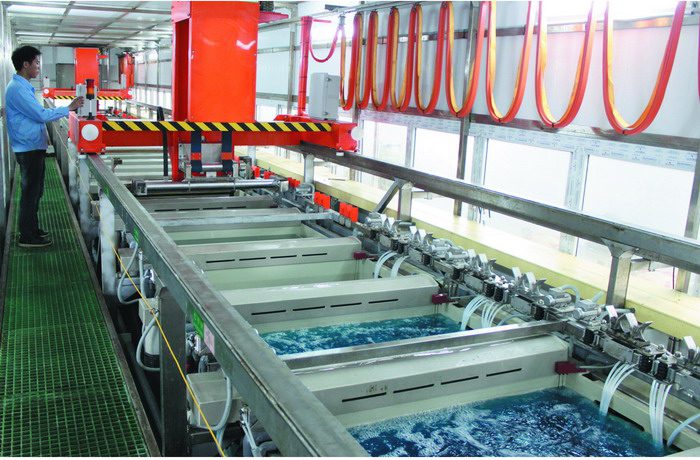
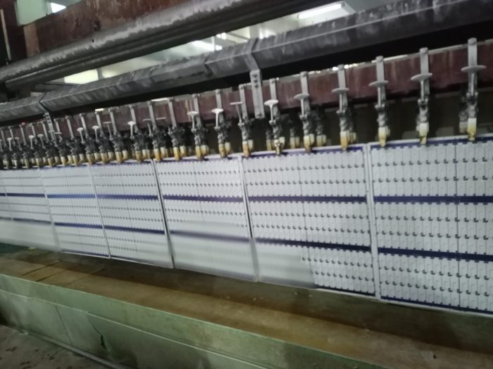
Following electroless plating, a thicker layer of copper is electroplated onto the hole walls to ensure reliable electrical connectivity and mechanical strength. According to IPC standards, the copper thickness for through-hole vias is typically required to be greater than 18 micrometers (IPC Class 2 standard), while blind vias and microvias may have different requirements. IPC Class 3 standards impose even stricter requirements, often requiring a copper thickness of over 20 micrometers.

4. Surface Finishing
Finally, the plated vias undergo surface finishing to improve corrosion resistance and solderability. Common surface finishes include gold plating, tin plating, and organic solderability preservatives (OSP).
Design Considerations for Plated Vias
When designing plated vias, several factors must be considered to ensure performance and reliability. Here are some key considerations:
1. Hole Size and Aspect Ratio
Hole size and aspect ratio (the ratio of hole depth to diameter) are critical parameters in plated via design. Too small a hole size or too high an aspect ratio can lead to uneven plating, affecting electrical performance and mechanical strength. Generally, the aspect ratio should be less than 10, and ideally less than 6 when space permits. Higher aspect ratios increase manufacturing difficulty and the likelihood of defects. In special cases where space is extremely limited, aspect ratios of up to 15 can be achieved, but this significantly increases manufacturing challenges and risks.
2. Hole Spacing
Hole spacing refers to the distance between adjacent plated vias. Insufficient spacing can cause electrical interference or reduced mechanical strength, while excessive spacing may waste space. Generally, hole spacing should be greater than 0.5mm (edge-to-edge). Insufficient spacing can affect the PCB’s lifespan, especially in harsh environments, potentially leading to ion migration (ICD) issues.
3. Signal Integrity
In high-frequency circuits, plated via design is crucial for signal integrity. Proper via layout and sizing can minimize signal reflection and loss, ensuring stable high-frequency signal transmission.
4. Thermal Management
In high-power electronic devices, plated via design must consider thermal management. Optimizing via layout and size can improve heat dissipation efficiency and reduce PCB temperature.
Common Issues and Solutions for Plated Vias
Several issues may arise during the manufacturing and use of plated vias. Here are some common problems and their solutions:
1. Uneven Plating
Uneven plating can lead to unreliable electrical connections or insufficient mechanical strength. Solutions include optimizing plating parameters (e.g., current density and plating time) and improving hole wall cleaning processes.
2. Hole Wall Fractures
Hole wall fractures can cause electrical disconnections or reduced mechanical strength. Solutions include optimizing drilling processes, increasing copper plating thickness, and improving PCB material selection.
3. Insufficient Copper Thickness
Insufficient copper thickness is a major issue with many low-quality PCB manufacturers. Some problems may only become apparent after SMT soldering, revealing incomplete performance. The worst-case scenario is when issues go unnoticed after SMT soldering and only emerge after prolonged use in the final product. At this point, it becomes difficult to determine how many defective or underperforming products are in the hands of end customers. Therefore, ensuring that copper thickness meets IPC standards is crucial.
Final Treatment Methods for Plated Vias
There are several final treatment methods for plated vias, including resin plugging, ink plugging, solder mask plugging, and via tenting. The choice of treatment method affects the long-term quality and reliability of the PCB:
Resin Plugging: Offers the best long-term quality and is suitable for high-reliability applications, but it is more expensive.
Ink Plugging: Provides good quality and is suitable for general industrial products.
Solder Mask Plugging: Lower cost but inferior long-term quality compared to resin and ink plugging.
Via Tenting: The most cost-effective option but offers the lowest long-term quality, suitable for applications with low reliability requirements.
The choice of treatment method should consider cost, operating environment, and product reliability requirements.
Conclusion
Plated vias are an indispensable part of PCB design, playing vital roles in electrical connectivity, heat dissipation, mechanical support, and signal integrity. Through proper design and manufacturing, the performance and reliability of plated vias can be ensured, thereby improving the overall quality of PCBs.
As electronic technology continues to advance, the design and pcb manufacturing of plated vias will face more challenges and opportunities. By adopting new technologies and materials, we can further optimize the performance of plated vias to meet the demands of future electronic devices.
At sqpcb, we are committed to delivering high-quality PCBs that meet the highest industry standards. With 14 years of experience, we have built a reputation for reliability and excellence, ensuring that our customers receive products that perform flawlessly in even the most demanding applications.
FAQ
Q1: What is the standard copper thickness for plated vias?
A1: IPC Class 2 requires ≥18 μm; Class 3 requires ≥20 μm.
Q2: How are microvias produced?
A2: Microvias (<150 μm) are typically manufactured using laser drilling.
Q3: How can via quality be tested?
A3: Methods include cross-section analysis, resistance testing, and X-Ray inspection.
Q4: Why do some suppliers have poor via quality?
A4: Many reduce plating thickness to cut costs, compromising reliability.
Q5: What advantages does SQPCB offer for plated vias?
A5: SQPCB’s LDI imaging, automated inkjet systems, in-house lamination, and ENIG plating ensure superior yield, reliability, and controlled lead times.
- long board pcb
- Flexible PCBs
- Special PCB
- Express Printed Circuit Board
- Pcb Prototype
- LED PCB
- PCB
- Printed Circuit Board
- Pcb meaning
- Pcb manufacturer
- Rigid pcb board
- Rigid Flex PCB

 Quote
Quote
 E-mail