Why the Surface Treatment of Your PCB Matters More Than You Think
Every detail in PCB manufacturing is crucial. The right surface treatment is not just about aesthetics—it determines the reliability, performance, and lifespan of your circuit board. A wrong choice could lead to oxidation, poor soldering, weak solder joints, or even severe impacts on your PCBA.
What is the OSP Surface Treatment?
OSP (Organic Solderability Preservative) is a cost-effective, lead-free, and highly solderable surface treatment that is becoming the go-to choice for many manufacturers. But is it the right option for your PCB?
Some swear by it, while others avoid it.
This detailed analysis will help you understand whether OSP is the perfect choice or a potential risk for your next project.

OSP Surface Treatment
What is the OSP Process?
The Organic Solderability Preservative (OSP) process is a specialized chemical surface treatment used in PCB manufacturing. Its primary function is to prevent copper oxidation while ensuring a clean, solderable surface. Unlike metallic finishes such as ENIG (Electroless Nickel Immersion Gold) or HASL (Hot Air Solder Leveling), OSP applies a thin organic layer to protect every exposed copper pad on the PCB.
This organic layer completely dissolves during soldering, exposing the raw copper to form a strong bond.
How Does the OSP Process Work?
Copper Cleaning – The PCB undergoes a rigorous micro-etching process to remove oxidation and contaminants.
OSP Coating Application – A water-based organic compound is chemically deposited onto the exposed copper pads.
Curing Process – The coating is stabilized through precise thermal treatment, ensuring uniform coverage and durability until assembly.
Why is OSP Different from Other Surface Finishes?
Unlike other metallic finishes, OSP is extremely thin (typically 0.2–0.5µm) and does not alter the flatness of the PCB. This makes it an excellent choice for fine-pitch components and high-density PCB designs.
Pros of the OSP Process
Cost-Effective and Budget-Friendly
OSP is one of the most economical PCB surface finishes available. Compared to ENIG or HASL, OSP requires fewer raw materials and a simpler process, reducing both production costs and environmental impact. For example, if the cost of OSP is 5 RMB per square meter, lead-free HASL costs 20 RMB per square meter, and ENIG with 2U gold thickness costs 160 RMB per square meter.
Eco-Friendly and Lead-Free
With global regulations like RoHS (Restriction of Hazardous Substances) in place, many manufacturers are shifting toward environmentally friendly alternatives. OSP:
Uses no heavy metals (unlike ENIG, which contains nickel).
Reduces waste through a water-based chemical process.
Complies with global green standards for electronics manufacturing.
Excellent Solderability
OSP provides an exceptionally clean and highly solderable copper surface. It is particularly well-suited for reflow soldering in SMT (Surface Mount Technology) processes, ensuring strong and reliable solder joints.
Smooth and Flat Surface for High-Density PCBs
Unlike HASL, which can create uneven solder layers, OSP maintains the PCB’s flatness, making it ideal for:
Fine-pitch components
High-frequency applications
BGA (Ball Grid Array) and QFN (Quad Flat No-lead) packages
Cons of the OSP Process
Limited Durability and Short Shelf Life
OSP coatings degrade faster than metal-based finishes. Exposure to air, moisture, and handling can weaken the protective layer, making it unsuitable for long-term storage without soldering.
Sensitive to Handling and Oxidation
Unlike ENIG or immersion silver, OSP lacks a metallic barrier. This makes it:
Prone to scratches or damage during PCB assembly.
Less effective if exposed to multiple handling stages before soldering.
Struggles with Multiple Reflow Cycles
While OSP excels in single reflow processes, its protective layer may degrade during multiple soldering passes. If your PCB requires multiple reflow cycles, OSP may not provide consistent solderability.
Poor Performance in Harsh Environments
High humidity and extreme temperatures can accelerate OSP degradation.
Storage and handling conditions must be carefully controlled to maintain the finish’s effectiveness.
OSP vs. Other Surface Finishes: Which is Best?
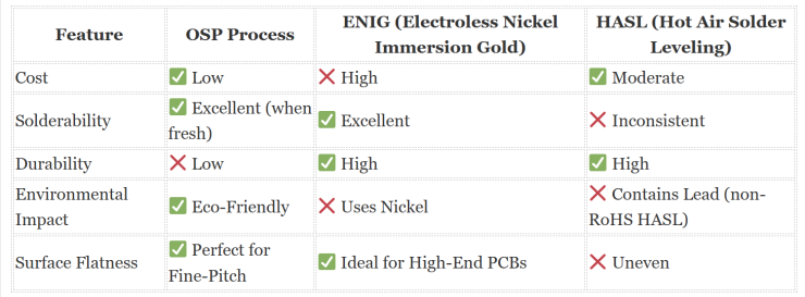
Choosing the Right Surface Finish Depends On:
✔ Budget constraints
✔ Storage and handling conditions
✔ Reflow soldering requirements
✔ PCB density and component layout
When to Choose the OSP Process for Your PCB
✅ Best for:
Cost-sensitive, high-volume production.
Single reflow processes (SMT assembly).
Short product lifecycles where soldering occurs quickly after PCB fabrication.
Fine-pitch components requiring an ultra-flat surface.
❌ Not Ideal for:
PCBs that require long shelf life before assembly.
Multi-reflow soldering cycles.
Electronics exposed to harsh environmental conditions.
Final Thoughts: Is OSP the Right Choice for Your PCB?
The OSP process is a powerful, cost-effective solution for high-volume PCB manufacturing. Its lead-free, environmentally friendly composition makes it an attractive alternative to more expensive finishes like ENIG.
However, its short shelf life and sensitivity to handling mean that not every PCB is suited for OSP. If your board will be exposed to multiple reflow cycles, harsh conditions, or long-term storage, alternatives like ENIG or HASL may be a better fit.
Choosing the right PCB surface finish is more than just a cost decision—it’s about performance, durability, and manufacturing efficiency. Consider your production needs, assembly process, and long-term reliability to determine if OSP is the right finish for your next PCB design
our linkedin sqpcb.com

- long board pcb
- Flexible PCBs
- Special PCB
- Express Printed Circuit Board
- Pcb Prototype
- LED PCB
- PCB
- Printed Circuit Board
- Pcb meaning
- Pcb manufacturer
- Rigid pcb board
- Rigid Flex PCB
 Quote
Quote
 E-mail