SSD PCBs: The Backbone of Solid State Drives
Solid-State Drives (SSDs) have revolutionized the data storage industry by providing faster, more reliable alternatives to traditional hard drives. At the heart of every SSD lies a crucial component: the Printed Circuit Board (PCB). The PCB in an SSD connects all the electrical components and ensures proper functionality, data storage, and retrieval processes. This article will explore the importance of SSD PCBs, the types of PCBs used in SSDs, their design, and the manufacturing process.
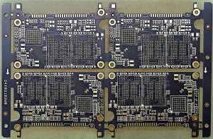
SSD PCBs
What is an SSD PCB?
An SSD PCB is a circuit board used in Solid-State Drives to connect the NAND flash memory chips, controller chips, and other components necessary for the drive’s operation. Unlike traditional hard drives, which rely on mechanical components like spinning disks and read/write heads, SSDs use flash memory to store data, making them faster and more durable.
The primary function of the SSD PCB is to facilitate communication between the various components, including NAND flash memory, DRAM (if used), and the controller. The quality and design of the SSD PCB directly impact the performance, speed, and longevity of the SSD.
Key Components of an SSD PCB
An SSD PCB contains several key components that work together to enable data storage and retrieval. Understanding these components is essential to grasp how an SSD functions.
1. NAND Flash Memory Chips
NAND flash memory is the core storage medium in an SSD. The NAND flash memory is responsible for storing all the data on the drive. These chips are organized in blocks and pages, and data is written to the memory in pages and read from the memory in blocks. NAND flash is non-volatile, meaning it retains data even when the power is turned off.
There are several types of NAND flash memory, including SLC (Single-Level Cell), MLC (Multi-Level Cell), TLC (Triple-Level Cell), and QLC (Quad-Level Cell). The choice of NAND flash affects the SSD’s performance, endurance, and cost. SLC provides the highest performance and longest lifespan but is more expensive, while QLC offers a higher capacity at a lower cost but with a reduced lifespan and performance.
2. Controller Chip
The controller chip is the brain of the SSD, managing the data flow between the NAND flash memory and the system. It handles tasks like wear leveling (distributing data evenly across the memory cells to extend their lifespan), garbage collection (removing unused data), and error correction. The controller chip is responsible for ensuring the SSD operates efficiently and reliably.
A high-quality controller chip can significantly improve an SSD’s performance, while a low-quality one can cause bottlenecks and reduce the drive’s overall speed.
3. DRAM (Dynamic Random Access Memory)
Some SSDs feature DRAM as a cache memory, which speeds up read and write operations. DRAM temporarily stores frequently accessed data, allowing the controller to retrieve it faster than accessing the NAND flash memory directly. SSDs with DRAM are typically faster than those without, but they also tend to be more expensive. DRAM is particularly useful for applications requiring high-speed data processing, such as gaming and video editing.
4. Power Management ICs
Power management ICs (PMICs) are essential for ensuring that the SSD receives stable power. These ICs manage voltage regulation, preventing fluctuations that could damage the components. PMICs are especially important in high-performance SSDs, which may consume more power during heavy workloads.
5. Connector Interface
The connector interface is the physical connection between the SSD and the host system (such as a computer or server). Common SSD interfaces include SATA, PCIe, and M.2. PCIe and M.2 interfaces offer significantly higher data transfer speeds compared to SATA, which is why PCIe-based SSDs are becoming the preferred choice for high-performance computing tasks.
Types of SSD PCBs
There are several types of SSD PCBs, each designed to meet different performance, size, and application requirements. The two most common types of SSD PCBs are:
1. SATA SSD PCB
SATA (Serial Advanced Technology Attachment) SSDs use the same interface as traditional hard drives but with the advantages of SSD technology. The SATA interface provides a data transfer rate of up to 600 MB/s, which is much faster than HDDs. SATA SSD PCBs are often used in consumer-grade SSDs for general-purpose storage.
SATA SSD PCBs are typically 2.5-inch form factor, making them compatible with most laptops and desktop computers. They use the same SATA data and power connectors as HDDs, making them easy to integrate into existing systems.
2. PCIe SSD PCB
PCIe (Peripheral Component Interconnect Express) SSDs are designed for higher performance and faster data transfer rates. The PCIe interface allows data transfer speeds of up to 7,000 MB/s or more, depending on the version (PCIe 3.0, 4.0, or 5.0) and the number of lanes (x1, x4, x8, x16).
PCIe SSD PCBs come in various form factors, including M.2, U.2, and add-in card (AIC). M.2 is the most common form factor, providing compact storage for ultrabooks and high-performance desktops. PCIe SSDs are typically used in professional and enterprise applications requiring high-speed data access, such as gaming, data centers, and video editing.
Designing an SSD PCB
The design of an SSD PCB is crucial to the performance, reliability, and efficiency of the drive. The design process involves several key considerations, including:
1. Signal Integrity
Signal integrity is critical to maintaining the speed and accuracy of data transfer between the controller and NAND flash memory. Proper layout and routing of traces are essential to minimize signal loss, electromagnetic interference (EMI), and crosstalk between signals. High-frequency signals are particularly susceptible to degradation, so the design must account for these factors.
2. Thermal Management
SSDs, especially high-performance ones, generate heat during operation. Efficient thermal management is crucial to prevent overheating and ensure the longevity of the components. Cooling solutions such as heat sinks, thermal pads, and proper PCB layout can help dissipate heat effectively.
3. Component Placement
The placement of components on the PCB is another critical design consideration. Components must be arranged to optimize space, minimize trace length, and ensure proper heat dissipation. Additionally, the layout must allow for efficient power delivery and signal routing.
4. Manufacturing Considerations
Once the design is complete, the PCB must be manufactured to precise specifications. This includes selecting appropriate materials for the substrate (usually FR4), ensuring proper layer stacking for multi-layer boards, and using precise manufacturing techniques to ensure the PCB meets the required electrical and mechanical standards.
Manufacturing Process of SSD PCBs
The manufacturing process of SSD PCBs involves several stages, each requiring precision and care to ensure the final product performs optimally. The key steps include:
1. PCB Fabrication
The fabrication process begins with creating the PCB layers, which are typically made from copper-clad laminates. The copper layers are etched to form the electrical traces that connect the components. Multi-layer boards may require the use of specialized processes, such as via-hole drilling and lamination, to create the necessary connections between layers.
2. Component Assembly
After the PCB is fabricated, components such as NAND flash chips, controller chips, and DRAM (if applicable) are mounted onto the PCB using surface-mount technology (SMT) or through-hole mounting, depending on the component type. SMT is the preferred method for most SSD PCBs due to its high-speed assembly and compact nature.
3. Testing and Quality Control
Once assembled, the SSD PCB undergoes various tests to ensure its functionality, including electrical testing, thermal testing, and performance testing. The finished PCB must meet rigorous quality control standards to ensure it will perform as expected.
Conclusion
The PCB is the heart of every SSD, connecting the critical components and enabling the drive to deliver high-speed data storage and retrieval. Whether you’re designing a consumer-grade SATA SSD or a high-performance PCIe SSD, the quality and design of the PCB play a significant role in the drive’s overall performance and reliability. Understanding the components, design considerations, and manufacturing process of SSD PCBs can help optimize your storage solutions and ensure the highest quality for your applications.

- long board pcb
- Flexible PCBs
- Special PCB
- Express Printed Circuit Board
- Pcb Prototype
- LED PCB
- PCB
- Printed Circuit Board
- Pcb meaning
- Pcb manufacturer
- Rigid pcb board
- Rigid Flex PCB
 Quote
Quote
 E-mail