Blank Printed Circuit Board: A Comprehensive Guide
Introduction
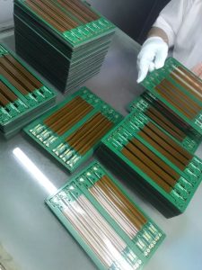
A blank printed circuit board (PCB) is the foundation of all electronic devices. It is an essential component that serves as the base for assembling electronic circuits, connecting various components such as resistors, capacitors, and integrated circuits (ICs). A blank PCB does not yet have components soldered onto it, but it contains copper traces and layers that form the electrical pathways.
This article explores what a blank PCB is, its structure, materials, manufacturing process, applications, and future trends in PCB technology.
Blank Printed Circuit Board
What is a Blank Printed Circuit Board?
A blank PCB refers to an unpopulated circuit board that contains conductive pathways (traces) but lacks mounted electronic components. It serves as the initial stage of PCB assembly, where components will later be soldered to create a functioning electronic circuit.
Blank PCBs come in various forms, depending on their design and application, including:
- Single-layer PCBs – Have a single copper layer on one side of the substrate.
- Double-layer PCBs – Feature copper layers on both sides of the board.
- Multi-layer PCBs – Contain multiple copper layers laminated together for complex electronic designs.
Structure of a Blank PCB
A blank PCB is made up of multiple layers that contribute to its electrical and mechanical properties. The main layers include:
1. Substrate (Base Material)
The substrate is the foundation of the PCB and provides structural support. Common materials used include:
- FR4 (Fiberglass Reinforced Epoxy) – The most widely used material, offering excellent electrical insulation and mechanical strength.
- Metal Core (Aluminum, Copper) – Used in high-power applications requiring superior heat dissipation.
- Ceramic Substrate – Ideal for high-frequency and high-temperature environments.
2. Copper Layer
The copper layer forms the conductive traces that connect components. The thickness of the copper layer varies based on the current-carrying requirements of the PCB, typically measured in ounces per square foot (e.g., 1oz, 2oz, 3oz).
3. Solder Mask
The solder mask is a protective layer applied over the copper traces to prevent oxidation, short circuits, and soldering errors. It is commonly green but can also be red, blue, black, or white.
4. Silkscreen Layer
The silkscreen layer is used to print component labels, part numbers, and reference markings on the PCB for easy assembly and identification.
5. Via Holes
Vias are small drilled holes that connect different PCB layers. There are three types of vias:
- Through-Hole Vias – Extend through the entire PCB.
- Blind Vias – Connect an outer layer to an inner layer without going through the entire board.
- Buried Vias – Connect inner layers only, without appearing on the outer surface.
Manufacturing Process of a Blank PCB
Step 1: Design and Layout
Engineers use PCB design software such as Altium Designer, Eagle, or KiCad to create a circuit layout, defining trace routes and layer configurations.
Step 2: Material Selection
The appropriate substrate and copper thickness are chosen based on the application requirements, including heat resistance and electrical conductivity.
Step 3: Printing the Circuit Pattern
The PCB design is transferred onto the copper-clad substrate using one of the following methods:
- Photoengraving (UV light exposure on a photosensitive layer)
- Screen Printing (Ink-based pattern transfer)
- Laser Direct Imaging (LDI) (Precision laser printing)
Step 4: Etching
Unwanted copper is removed using chemical etching, leaving behind only the designed circuit traces.
Step 5: Drilling Holes
Holes are drilled for vias, mounting pads, and component leads using precision CNC drilling machines.
Step 6: Plating and Surface Finish
Copper plating is applied to drilled holes to improve conductivity. Common surface finishes include:
- HASL (Hot Air Solder Leveling) – Cost-effective but less suitable for fine-pitch components.
- ENIG (Electroless Nickel Immersion Gold) – Provides excellent solderability and corrosion resistance.
- OSP (Organic Solderability Preservative) – A lead-free option used for environmental compliance.
Step 7: Solder Mask and Silkscreen Application
The solder mask and silkscreen layers are added for protection and component labeling.
Step 8: Final Inspection and Quality Control
The blank PCB undergoes electrical testing, X-ray inspection, and visual checks to ensure compliance with design specifications.
Applications of Blank PCBs
Blank PCBs are used in a wide range of industries, including:
1. Consumer Electronics
- Smartphones, laptops, and tablets
- Televisions and home automation devices
2. Automotive Electronics
- Engine control units (ECUs)
- Infotainment and navigation systems
- Electric vehicle (EV) power management systems
3. Industrial and IoT Devices
- Factory automation and robotics
- Sensor networks and smart home devices
- Industrial power control systems
4. Medical Equipment
- Patient monitoring systems
- MRI and ultrasound machines
- Implantable medical devices
5. Aerospace and Defense
- Radar and communication systems
- Satellite electronics
- Military-grade computing systems
Future Trends in Blank PCB Technology
1. High-Density Interconnect (HDI) PCBs
- Use of microvias and ultra-thin layers for compact designs.
- Essential for advanced consumer electronics and 5G applications.
2. Flexible and Rigid-Flex PCBs
- Integration of flexible circuits with rigid PCBs for wearables and foldable devices.
- Enables high-performance compact designs in automotive and aerospace sectors.
3. Environmentally Friendly PCBs
- Development of lead-free and biodegradable PCB materials.
- Use of recyclable substrates to reduce e-waste.
4. AI-Assisted PCB Design
- Machine learning algorithms optimizing PCB layouts for better signal integrity.
- Predictive analysis reducing manufacturing defects and enhancing efficiency.
5. Embedded Components in PCBs
- Integration of passive and active components within PCB layers.
- Improves performance and miniaturization for advanced electronics.
Conclusion
A blank printed circuit board (PCB) is the backbone of modern electronic devices, providing the essential platform for assembling electrical circuits. From design and material selection to manufacturing and applications, blank PCBs play a crucial role in various industries, including consumer electronics, automotive, medical, industrial automation, and aerospace.
With continuous advancements in high-density interconnect, flexible PCBs, AI-driven designs, and eco-friendly materials, the future of blank PCBs promises even greater efficiency, performance, and sustainability in electronic product development. Understanding blank PCBs is essential for engineers, manufacturers, and businesses looking to innovate in the ever-evolving world of electronics.

- long board pcb
- Flexible PCBs
- Special PCB
- Express Printed Circuit Board
- Pcb Prototype
- LED PCB
- PCB
- Printed Circuit Board
- Pcb meaning
- Pcb manufacturer
- Rigid pcb board
- Rigid Flex PCB
 Quote
Quote
 E-mail