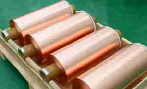
Copper Foil for PCB Lamination: Properties, Types, and Applications
Introduction
Copper foil is one of the most essential materials used in PCB (Printed Circuit Board) lamination, serving as the primary conductive layer that forms circuit pathways. It is laminated onto prepreg and core materials during the PCB manufacturing process, enabling the creation of high-density, high-speed, and reliable electrical connections.
The selection of copper foil type, thickness, surface treatment, and adhesion properties plays a crucial role in determining PCB performance, manufacturing efficiency, and long-term reliability. This article explores the properties, types, lamination process, and best practices for selecting copper foil for PCB applications.

Copper Foil for PCB Lamination
Key Properties of Copper Foil in PCB Manufacturing
1. Electrical Conductivity
- Copper has high electrical conductivity (59.6 × 10⁶ S/m), ensuring low resistance and efficient signal transmission.
- A uniform and defect-free copper surface is critical for high-frequency and high-speed PCBs.
2. Thermal Conductivity
- Copper’s high thermal conductivity helps dissipate heat efficiently, reducing the risk of overheating in power electronics and high-speed circuits.
- Thicker copper foils are used for high-current applications to improve heat management.
3. Adhesion Strength
- Copper foil must have strong adhesion to prepreg materials to ensure structural stability.
- Surface treatments such as oxide coatings and chemical roughening improve bonding strength and prevent delamination.
4. Flexibility and Mechanical Strength
- Copper foil needs sufficient flexibility for flex and rigid-flex PCBs.
- Higher mechanical strength is required for multilayer PCBs to withstand the stresses of lamination and thermal cycling.
Types of Copper Foil Used in PCB Lamination
Copper foil is classified based on manufacturing processes and surface treatments, each with unique characteristics that influence PCB performance.
1. Electrodeposited (ED) Copper Foil
- Manufacturing Process: Produced by electroplating copper onto a rotating drum.
- Key Features:
- Lower cost and widely used in standard PCB applications.
- Grain structure: Columnar, providing moderate flexibility.
- Higher surface roughness, which improves adhesion but may affect high-frequency signal transmission.
- Application:
- Rigid PCBs, consumer electronics, and general-purpose boards.
2. Rolled Annealed (RA) Copper Foil
- Manufacturing Process: Created by rolling and annealing solid copper sheets.
- Key Features:
- Fine and uniform grain structure, improving mechanical flexibility.
- Smoother surface, reducing signal loss in high-frequency applications.
- Higher cost than ED copper.
- Application:
- Flexible PCBs, HDI PCBs, and RF/microwave circuits.
3. Reverse-Treated (RTF) Copper-Foil
- Manufacturing Process: Similar to ED copper but with roughness applied on both sides.
- Key Features:
- Improved adhesion on both sides, reducing risk of delamination.
- Balanced surface roughness, optimizing signal integrity.
- Application:
- High-layer count PCBs, HDI, and high-reliability applications.
4. Low-Profile and Ultra-Low-Profile Copper Foil
- Manufacturing Process: Specially processed ED copper with minimal surface roughness.
- Key Features:
- Extremely smooth surface, reducing signal attenuation.
- Improves impedance control for high-speed designs.
- Application:
- 5G, RF/microwave, and high-speed data transmission PCBs.
5. High-Tensile Copper Foil
- Designed for: Applications requiring high mechanical strength and durability.
- Used in: Automotive, aerospace, and industrial PCBs.
Copper Foil Thickness Standards for PCBs
Copper-foil is available in various thickness grades, measured in ounces per square foot (oz/ft²).
| Copper Thickness | Metric (µm) | Application |
|---|---|---|
| 0.5 oz/ft² | ~17 µm | HDI PCBs, fine-line circuits |
| 1 oz/ft² | ~35 µm | Standard multilayer PCBs |
| 2 oz/ft² | ~70 µm | High-power PCBs, improved thermal management |
| 3 oz/ft² | ~105 µm | Heavy copper PCBs for industrial/power applications |
| 4 oz/ft²+ | ~140+ µm | Power electronics, automotive, aerospace PCBs |
Copper Foil in the PCB Lamination Process
1. Preparation and Cleaning
- Copper-foil is cleaned and treated to remove oxidation and contaminants.
- Surface roughening or chemical treatments enhance adhesion to prepreg layers.
2. Layer Stacking and Alignment
- Copper foil is aligned with prepreg and core layers following the PCB’s stack-up design.
- Proper alignment prevents layer shifting and registration errors.
3. High-Temperature and High-Pressure Lamination
- The lamination press bonds copper-foil to prepreg under heat (130–200°C) and pressure (200–400 psi).
- Resin from prepreg flows and cures, ensuring a strong bond between copper and dielectric layers.
4. Cooling and Stress Stabilization
- Gradual cooling under controlled pressure reduces stress buildup and prevents warping.
- Improper cooling may cause delamination or thickness variations.
5. Post-Lamination Processes
- Laminated copper layers are drilled, etched, and plated to form circuit patterns.
- X-ray or optical inspection checks for bonding defects or voids.
Best Practices for Copper-Foil Selection and Lamination
- Choose the right copper-foil type based on the PCB’s application (ED for standard PCBs, RA for flex circuits, and low-profile for high-frequency designs).
- Ensure proper surface treatment to enhance adhesion and prevent delamination.
- Match copper foil thickness to the PCB’s electrical and thermal requirements.
- Use symmetrical copper distribution to reduce stress and prevent warping.
- Control lamination temperature and pressure to ensure uniform resin flow and proper bonding.
- Implement a controlled cooling process to minimize internal stress and maintain dimensional stability.
- Perform quality inspections to check for adhesion strength, surface defects, and uniformity.
Conclusion
Copper foil is an essential material in PCB lamination, directly affecting electrical performance, thermal management, and mechanical stability. Choosing the right copper type, thickness, and surface treatment ensures strong adhesion, minimal signal loss, and long-term reliability.
By optimizing the lamination process, material selection, and quality control, PCB manufacturers can produce high-performance multilayer boards for applications ranging from consumer electronics to high-frequency, automotive, and aerospace industries. With continuous advancements in copper foil technology, the future of PCBs will support even higher speeds, greater reliability, and enhanced miniaturization for next-generation electronic devices.
- long board pcb
- Flexible PCBs
- Special PCB
- Express Printed Circuit Board
- Pcb Prototype
- LED PCB
- PCB
- Printed Circuit Board
- Pcb meaning
- Pcb manufacturer
- Rigid pcb board
- Rigid Flex PCB

 Quote
Quote
 E-mail