What is PWB? Understanding Printed Wiring Boards and Their Role in Electronics
Introduction
In the field of electronics manufacturing, the terms PWB (Printed Wiring Board) and PCB (Printed Circuit Board) are often used interchangeably. However, there are some differences between them in historical context and usage. Understanding what a PWB is, how it differs from a PCB, and its importance in electronic design and production is essential for engineers, manufacturers, and industry professionals.
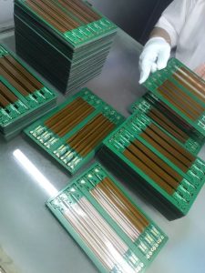
A Printed Wiring Board (PWB) is a board that provides electrical connections between different components without mounted electronic elements. It consists of conductive pathways, usually made of copper, printed or etched onto an insulating substrate. PWBs form the foundation for electronic devices, ensuring stable and reliable connections.
This article will explore the definition, structure, manufacturing process, applications, and differences between PWBs and PCBs, providing a comprehensive understanding of this crucial electronic component.
What is PWB
What is a Printed Wiring Board (PWB)?
A Printed Wiring Board (PWB) is a substrate that contains copper traces designed to connect different electronic components. Unlike a Printed Circuit Board (PCB), a PWB does not include mounted components such as resistors, capacitors, or integrated circuits (ICs). Instead, it serves as the base onto which components are later assembled.
PWBs are essential in electronics manufacturing, serving as the structural foundation for nearly all electronic devices. They enable precise electrical routing, ensuring signals are transmitted efficiently between various parts of a circuit.
Basic Structure of a PWB
A typical PWB consists of the following layers:
- Substrate (Base Material) – Usually made of FR-4 (fiberglass-reinforced epoxy), polyimide, or other insulating materials, providing mechanical strength.
- Copper Layers – Thin layers of copper are etched or printed to create conductive pathways that connect different circuit points.
- Solder Mask – A protective layer that covers the copper traces to prevent oxidation and short circuits.
- Silkscreen Layer – A printed layer used for component markings, labels, and identifiers to aid in assembly and troubleshooting.
PWB vs. PCB: Understanding the Difference
Many people use PWB and PCB interchangeably, but there are key differences between them:
| Aspect | PWB (Printed Wiring Board) | PCB (Printed Circuit Board) |
|---|---|---|
| Definition | A board with only wiring (copper traces) but no mounted components. | A complete board with wiring and electronic components. |
| Usage Context | More commonly used in early electronics and aerospace industries. | Widely used in modern electronics manufacturing. |
| Manufacturing Stage | A pre-assembly stage before electronic components are added. | A fully assembled and functional circuit board. |
| Complexity | Typically simpler, used in basic circuits. | Can be highly complex, including multilayer and HDI designs. |
In the past, PWB was the preferred term, especially in industries like aerospace and defense. However, as electronics evolved, PCB became the dominant term for both pre-assembly and fully assembled boards.
PWB Manufacturing Process
The manufacturing of a PWB involves several key steps to ensure reliability and accuracy in electrical connections. Below is an overview of the PWB fabrication process:
1. Design & Layout
- Engineers design the PWB using computer-aided design (CAD) software such as Altium, Eagle, or KiCad.
- The layout is optimized for signal integrity, power distribution, and manufacturability.
2. Material Selection
- The substrate material is chosen based on thermal stability, mechanical strength, and electrical properties.
- Common materials include FR-4, polyimide (for flexible PWBs), and metal-core substrates.
3. Copper Layer Deposition
- Thin sheets of copper foil are bonded to the substrate.
- In multilayer PWBs, multiple copper layers are stacked and laminated together.
4. Etching & Circuit Patterning
- A chemical etching process is used to remove unwanted copper, leaving behind the desired circuit traces.
- Alternatively, additive printing techniques can be used for fine-line PWBs.
5. Drilling & Via Formation
- Mechanical or laser drilling creates holes (vias) for electrical connections between layers.
- Common via types:
- Through-hole vias – Connect top to bottom layers.
- Blind/Buried vias – Connect internal layers without reaching the outer surface.
6. Surface Treatment & Solder Mask Application
- Surface finishes such as HASL (Hot Air Solder Leveling), ENIG (Electroless Nickel Immersion Gold), or OSP (Organic Solderability Preservative) are applied for better solderability.
- A solder mask is applied to protect copper traces from oxidation and shorts.
7. Quality Control & Testing
- Optical and electrical tests such as Automated Optical Inspection (AOI) and Flying Probe Testing are performed to ensure manufacturing accuracy.
- Any defects are corrected before assembly begins.
Applications of PWBs
Printed Wiring Boards (PWBs) are used in a wide range of electronic applications, including:
- Consumer Electronics – Smartphones, tablets, TVs, and home appliances.
- Automotive Electronics – Engine control units (ECUs), navigation systems, and sensors.
- Medical Devices – Imaging equipment, patient monitoring systems, and diagnostic tools.
- Aerospace & Defense – High-reliability circuits for avionics, radars, and satellite systems.
- Industrial Equipment – Control panels, automation systems, and power management devices.
PWBs are critical in every industry where reliable electrical connections are required.
Future Trends in PWB Technology
As technology advances, PWBs are evolving to meet the demands of miniaturization, higher speed, and better durability. Some key trends in PWB technology include:
- Flexible and Rigid-Flex PWBs – Used in foldable devices and wearable technology.
- High-Density Interconnect (HDI) PWBs – Allow for smaller, more powerful electronic designs.
- Embedded Components in PWBs – Reducing the need for external surface-mounted components.
- Eco-Friendly Manufacturing – Adoption of lead-free and recyclable materials to comply with environmental regulations.
Conclusion
A Printed Wiring Board (PWB) is the foundation of modern electronics, providing essential electrical connections before component assembly. While the term PWB was historically used to differentiate between circuit boards with and without components, PCB is now the dominant term in the industry.
Understanding the structure, manufacturing process, and applications of PWBs helps engineers and manufacturers optimize designs for performance and reliability. As technology advances, PWBs will continue to play a crucial role in the development of next-generation electronic devices.
By ensuring precise fabrication and quality control, manufacturers can produce PWBs that meet the highest industry standards, enabling innovation in consumer electronics, automotive systems, aerospace applications, and beyond.

- long board pcb
- Flexible PCBs
- Special PCB
- Express Printed Circuit Board
- Pcb Prototype
- LED PCB
- PCB
- Printed Circuit Board
- Pcb meaning
- Pcb manufacturer
- Rigid pcb board
- Rigid Flex PCB
 Quote
Quote
 E-mail