Copper Coin PCB: Design, Benefits, and Applications
Introduction
With the increasing demand for high-power and high-thermal-performance electronic devices, Copper Coin PCBs have become a vital solution for thermal management and power stability. Unlike standard PCBs, Copper Coin PCBs integrate a solid copper inlay to enhance heat dissipation and electrical conductivity, making them ideal for LEDs, power electronics, automotive applications, and high-frequency circuits.
This article explores what Copper Coin PCBs are, their structure, advantages, manufacturing process, and key applications in modern electronics.
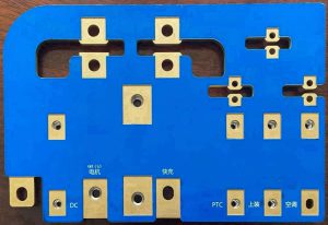
Copper Coin PCB
What is a Copper Coin PCB?
A Copper Coin PCB is a high-performance printed circuit board (PCB) that incorporates a solid copper inlay (also known as a “copper coin”) embedded into the PCB substrate. This structure significantly improves thermal conductivity and electrical performance, addressing the challenges of heat dissipation in power-intensive components.
Unlike traditional PCBs that rely on thermal vias or heat sinks, Copper Coin PCBs directly transfer heat from high-power components to the copper inlay, reducing thermal resistance and ensuring stable operation.
Types of Copper Coin PCBs
There are several types of Copper Coin PCBs based on the integration of copper inlays:
| Type | Description | Best Applications |
|---|---|---|
| Embedded Copper Coin PCB | Copper coin is fully embedded inside the PCB layers. | High-power modules, LED lighting |
| Press-Fit Copper Coin PCB | Copper coin is press-fitted into a pre-milled slot on the PCB. | Automotive electronics, industrial power supplies |
| Soldered Copper Coin PCB | Copper coin is soldered directly onto the PCB surface. | RF circuits, high-frequency devices |
Why Use a Copper Coin PCB?
1. Superior Thermal Conductivity
✔ Copper Coin PCBs efficiently dissipate heat, preventing overheating of power-intensive components.
✔ Reduces hot spots and temperature variations, ensuring stable performance.
2. Increased Electrical Performance
✔ Copper inlays provide low-resistance power transmission, improving overall circuit efficiency.
✔ Ideal for high-current applications where power loss must be minimized.
3. Enhanced Mechanical Strength
✔ The solid copper structure reinforces PCB durability, reducing mechanical stress.
✔ Suitable for harsh environments, including automotive and aerospace electronics.
4. Improved Signal Integrity
✔ Copper Coin PCBs offer better EMI shielding and impedance control, crucial for high-frequency circuits.
✔ Reduces parasitic inductance, improving signal transmission efficiency.
5. Long-Term Reliability
✔ Ensures stable electrical and thermal performance over extended operational periods.
✔ Minimizes the risk of component failure due to heat accumulation.
Manufacturing Process of PCBs with Copper Coin
The manufacturing process of Copper Coin PCBs requires high-precision techniques to integrate copper inlays into the PCB structure.
Step 1: PCB Design and Material Selection
- FR-4, High-Tg FR-4, Rogers, or Metal Core PCB (MCPCB) materials are commonly used.
- Copper inlay thickness (typically 1.5mm – 3.0mm) is selected based on power requirements.
Step 2: Milling and Copper Coin Placement
- Milling slots or cavities are created in the PCB substrate to accommodate the copper inlay.
- The copper coin is precision-cut and fitted into the prepared cavity.
Step 3: Lamination and Bonding
- High-pressure and high-temperature lamination fuses the PCB layers together.
- Prepreg materials are used to ensure secure copper integration.
Step 4: Drilling and Plating
- Through-holes and vias are drilled to establish electrical connections.
- Copper plating is applied to ensure conductivity between PCB layers.
Step 5: Surface Finishing and Testing
- ENIG (Electroless Nickel Immersion Gold), HASL, or OSP surface treatments are applied.
- Electrical and thermal conductivity tests verify the PCB’s performance.
Copper Coin PCB vs. Traditional Thermal Management Solutions
| Feature | Copper Coin PCB | Standard PCB with Thermal Vias | MCPCB (Metal Core PCB) |
|---|---|---|---|
| Thermal Conductivity | Excellent | Moderate | High |
| Power Handling Capacity | High | Low | High |
| Design Flexibility | High | High | Limited |
| Weight and Thickness | Moderate | Thin | Thicker |
| Manufacturing Cost | Higher | Lower | Moderate |
Copper Coin PCBs offer superior heat dissipation and power efficiency compared to standard PCBs and MCPCBs, making them a preferred choice for high-power applications.
Key Applications of PCBs with Copper Coin
Copper Coin PCBs are widely used in high-performance and power-intensive electronic devices.
1. LED Lighting and Display Technology
- Used in high-power LED lighting systems to dissipate heat efficiently.
- Prevents luminous decay and color shifting in LED modules.
2. Automotive and Electric Vehicles (EVs)
- Supports battery management systems (BMS), power inverters, and ECU circuits.
- Ensures thermal stability in extreme temperature conditions.
3. Telecommunications and 5G Infrastructure
- Found in 5G base stations, RF power amplifiers, and satellite communications.
- Enhances signal transmission and EMI shielding.
4. Industrial Power Electronics
- Used in high-current power supplies, motor controllers, and energy storage systems.
- Improves power efficiency and heat management in industrial applications.
5. Aerospace and Military Electronics
- Essential for radar systems, avionics, and defense communication networks.
- Withstands harsh environmental conditions and high-frequency operations.
Challenges in Manufacturing the PCBs With Copper Coin
Despite their advantages, PCBs with Copper Coin present several manufacturing challenges:
❌ Complex Manufacturing Process – Requires precise milling, copper inlay integration, and lamination techniques.
❌ Higher Production Costs – The cost of copper inlays and precision processing is higher than standard PCBs.
❌ Thermal Expansion Mismatch – Different expansion rates of copper and PCB materials must be managed to prevent mechanical stress.
❌ Limited PCB Thickness Options – Thicker copper inlays increase overall PCB thickness, affecting compact designs.
To overcome these challenges, high-precision PCB manufacturers use advanced milling, laser drilling, and automated inspection techniques.
Conclusion
Copper Coin PCBs provide superior thermal management, enhanced electrical performance, and improved reliability for high-power and high-frequency electronic applications. They are widely used in LED lighting, automotive, telecommunications, industrial, and aerospace electronics.
With advanced manufacturing techniques, PCBs with Copper Coin offer a highly effective solution for heat dissipation and power stability, ensuring long-term circuit reliability in demanding applications.
At Shuoqiang Electronics, we specialize in high-performance PCBs with Copper Coin manufacturing, providing custom solutions for thermal management and power optimization. Contact us today for precision-engineered PCBs with Copper Coin!
our linkedin sqpcb.com

- long board pcb
- Flexible PCBs
- Special PCB
- Express Printed Circuit Board
- Pcb Prototype
- LED PCB
- PCB
- Printed Circuit Board
- Pcb meaning
- Pcb manufacturer
- Rigid pcb board
- Rigid Flex PCB
 Quote
Quote
 E-mail