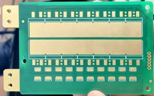
Understanding ENIG Gold Thickness in PCB Manufacturing
Electroless Nickel Immersion Gold (ENIG) is one of the most widely used surface finishes in printed circuit board (PCB) manufacturing. It provides excellent solderability, corrosion resistance, and a flat surface for component placement. A key factor in ENIG performance is the gold thickness, which directly impacts durability, reliability, and cost. In this article, we will explore the significance of ENIG gold thickness, industry standards, measurement methods, and best practices for achieving optimal results.

ENIG Gold Thickness
1. What is ENIG?
ENIG is a two-layer metallic coating applied to copper traces on a PCB. It consists of:
- Nickel Layer: Acts as a barrier to prevent copper migration and provides a base for gold deposition.
- Gold Layer: Protects the nickel from oxidation and ensures good solderability.
ENIG is preferred over other surface finishes due to its flatness, oxidation resistance, and long shelf life. It is extensively used in high-reliability applications, including aerospace, medical devices, and high-density interconnect (HDI) PCBs.
2. Importance of Gold Thickness in ENIG
The thickness of the immersion gold layer plays a critical role in the performance of ENIG-finished PCBs. Key reasons why gold thickness matters include:
2.1 Solderability and Wetting
A thin gold layer ensures that the underlying nickel is protected, but if it is too thin, oxidation may occur, leading to poor solderability. A proper gold thickness improves wetting performance, ensuring strong and reliable solder joints.
2.2 Corrosion Resistance
Gold is highly resistant to oxidation and tarnishing. A thicker gold layer provides better protection against environmental factors such as humidity, high temperatures, and chemical exposure.
2.3 Shelf Life of PCBs
PCBs with a thicker gold layer generally have a longer shelf life, making them suitable for applications where components are soldered months or even years after manufacturing.
2.4 Cost Considerations
Gold is an expensive material. While a thicker layer improves durability, excessive thickness increases costs without significant benefits. Manufacturers aim to balance thickness to ensure quality while keeping production costs competitive.
3. Standard ENIG Gold Thickness in PCB Manufacturing
The typical immersion gold thickness in ENIG-finished PCBs varies based on industry standards and application requirements. Below are some commonly followed guidelines:
| Standard/Specification | Gold Thickness (µin) | Gold Thickness (µm) |
|---|---|---|
| IPC-4552 (Industry Standard) | 2–4 µin | 0.05–0.10 µm |
| High-End PCBs (e.g., Aerospace, Medical) | 4–8 µin | 0.10–0.20 µm |
| Consumer Electronics | 1.5–3 µin | 0.04–0.08 µm |
| Automotive PCBs | 3–6 µin | 0.08–0.15 µm |
Most PCBs use 2–4 µin (0.05–0.10 µm) as the standard gold thickness, which provides a balance between cost and performance.
4. Methods for Measuring Gold Thickness
Manufacturers use various techniques to verify ENIG gold thickness to ensure compliance with industry standards. The most common measurement methods include:
4.1 X-Ray Fluorescence (XRF) Analysis
- A non-destructive technique that accurately measures gold thickness.
- Provides real-time feedback during production.
- Commonly used in PCB factories for quality control.
4.2 Scanning Electron Microscopy (SEM)
- Offers high-resolution imaging to analyze the gold and nickel layers.
- Used for advanced failure analysis and research.
4.3 Cross-Sectional Analysis
- A destructive method where the PCB is cut and analyzed under a microscope.
- Provides precise layer thickness measurements.
Manufacturers rely primarily on XRF analysis for in-line quality control due to its speed, accuracy, and non-destructive nature.
5. Common Issues Related to Gold Thickness
5.1 Too Thin Gold Layer (<2 µin / 0.05 µm)
- Leads to nickel oxidation, reducing solderability.
- Increases the risk of “black pad” defects, causing poor electrical connections.
- Shortens the shelf life of the PCB.
5.2 Too Thick Gold Layer (>8 µin / 0.20 µm)
- Increases costs without major benefits.
- Can lead to brittle solder joints, making them prone to fractures under mechanical stress.
- Causes gold embrittlement, leading to poor mechanical strength.
Maintaining an optimal thickness between 2–4 µin (0.05–0.10 µm) ensures good solderability, durability, and cost-effectiveness.
6. Best Practices for Controlling Gold Thickness in ENIG PCBs
To ensure consistent and high-quality ENIG coatings, PCB manufacturers follow these best practices:
✅ Precise Chemical Control: Maintaining proper gold bath chemistry ensures consistent deposition rates.
✅ Optimized Processing Time: Immersion time should be carefully controlled to avoid over-thick or under-thick deposits.
✅ Regular Thickness Testing: Using XRF measurement during production prevents deviations from required thickness.
✅ Supplier Quality Control: Working with reputable PCB manufacturers ensures compliance with IPC-4552 and other industry standards.
7. Conclusion
ENIG gold thickness is a crucial factor in determining the reliability, solderability, and cost-effectiveness of PCBs. While a minimum of 2 µin (0.05 µm) is necessary to prevent oxidation, excessive thickness above 8 µin (0.20 µm) can cause problems such as brittle solder joints and increased costs.
By following industry standards (IPC-4552), employing accurate thickness measurement methods (XRF), and optimizing production parameters, manufacturers can ensure high-quality PCBs with optimal performance.
For businesses looking to produce high-reliability PCBs with the right ENIG gold thickness, partnering with an experienced manufacturer like Shenzhen Shuoqiang Electronics ensures top-tier quality and cost-effective solutions.
our linkedin sqpcb.com
- long board pcb
- Flexible PCBs
- Special PCB
- Express Printed Circuit Board
- Pcb Prototype
- LED PCB
- PCB
- Printed Circuit Board
- Pcb meaning
- Pcb manufacturer
- Rigid pcb board
- Rigid Flex PCB

 Quote
Quote
 E-mail