what is the silk to solder mask clearance
- Introduction
- What is Silk to Solder Mask Clearance?
- Why is Silk to Solder Mask Clearance Important?
- How Equipment Precision Affects Minimum Silk to Solder Mask Clearance
- Recommended Silk to Solder Mask Clearance Guidelines
- Design Considerations for Proper Clearance
- How to Check Silk to Solder Mask Clearance in PCB Design Software
- Common Issues and Solutions
- Best Practices for Silk to Solder Mask Clearance
- Conclusion
- FAQs About Silk to Solder Mask Clearance
Introduction
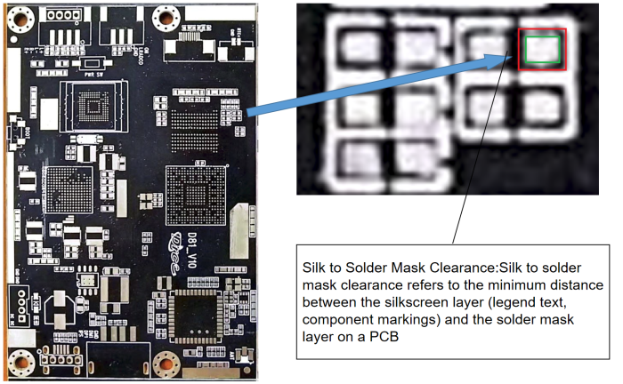
Silk to solder mask clearance: refers to the minimum distance between the silkscreen layer (legend text, component markings) and the solder mask layer on a PCB. it is a critical aspect of PCB (Printed Circuit Board) design, ensuring readability, manufacturing reliability, and component placement accuracy. Proper clearance prevents printing issues, misalignment, and short circuits, enhancing the overall quality and durability of the PCB.
Leading manufacturers such as SQPCB prioritize tight control of silkscreen and solder mask tolerances during fabrication, helping customers minimize defects and improve assembly yields.
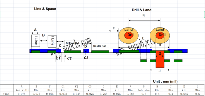
This article explores what silk to solder mask clearance is, its importance, recommended design guidelines, and best practices for achieving optimal PCB functionality. the follow sqpcb capbility show, the C2 is the solder mask clearance

silk to solder mask clearance
What is Silk to Solder Mask Clearance?
Silk to solder mask clearance refers to the minimum distance between the silkscreen layer (legend text, component markings) and the solder mask layer on a PCB. This clearance ensures that silkscreen printing does not overlap with solder pads, preventing printing errors, manufacturing defects, and potential short circuits. While some may consider solder mask clearance more critical, it’s important to note that many pads are opened directly over large copper areas—making silk to solder mask clearance just as essential for ensuring reliability and clarity in PCB design.

Key PCB Layers Involved:
Silkscreen Layer (Legend Layer) – Contains component labels, polarity indicators, and branding.
Solder Mask Layer – A protective layer that covers copper traces, leaving openings for soldering pads and vias.
Copper Layer – The conductive layer forming the PCB’s electrical pathways.
Why is Silk to Solder Mask Clearance Important?
1. Prevents Overlapping Issues
Ensures that silkscreen markings do not overlap with solder pads, preventing ink from covering critical soldering areas.
2. Improves PCB Readability
Proper clearance ensures clear text and component labeling, avoiding blurred, misprinted, or smudged markings.
3. Enhances Soldering Accuracy
Prevents silkscreen ink from interfering with solder joints, reducing the risk of poor solder connections and component misalignment.
4. Reduces Manufacturing Errors
Many PCB manufacturers remove silkscreen that overlaps with solder mask openings, which can lead to missing important component labels or design inconsistencies.
By utilizing in-house solde mask LDI imaging and silkscreen automation, SQPCB ensures precise registration between silk and mask layers—even on high-density and fast-turn PCBs.
How Equipment Precision Affects Minimum Silk to Solder Mask Clearance
The minimum silk to solder mask clearance is directly related to the alignment precision of the equipment used during PCB fabrication. Different types of exposure machines offer varying levels of registration accuracy:
Manual Exposure Machines rely on vacuum and film alignment, with typical alignment deviations of ±50–75μm. These machines are more prone to film shift and human error.
CCD Alignment Exposure Machines improve accuracy with optical positioning, usually achieving ±25–40μm precision, but still depend on film and vacuum.
LDI (Laser Direct Imaging) Exposure Machines offer the highest precision, down to ±10–15μm, thanks to direct digital imaging and automated registration—no film, no vacuum distortion. The direct imaging pcb normally is more statable
Similarly, the accuracy of silkscreen text depends on the method of application. Traditional screen printing may have deviations over 75μm due to mesh distortion and ink spreading. In contrast, automated inkjet legend printers can achieve text alignment within ±30μm, delivering better clarity and consistency.
At SQPCB, we’ve fully implemented inline LDI solder mask exposure systems and automated text inkjet printers. This investment dramatically improves layer-to-layer alignment, reduces printing defects, and ensures consistent, high-resolution legends—even on complex or dense PCB layouts.
Recommended Silk to Solder Mask Clearance Guidelines
The recommended clearance varies depending on PCB manufacturing capabilities and design complexity. The following values are commonly used in industry-standard PCB designs:
| Parameter | Recommended Clearance |
|---|---|
| Minimum Silk to Solder Mask Clearance | 0.15mm (6 mils) |
| Preferred Clearance | 0.2mm – 0.25mm (8-10 mils) |
| Minimum Silkscreen Text Height | 1.0mm (40 mils) |
| Minimum Silkscreen Line Width | 0.15mm (6 mils) |
| Silkscreen to Pad Clearance | 0.2mm (8 mils) or more |
Design Considerations for Proper Clearance
1. Define Proper Silkscreen Boundaries
Ensure that silkscreen text and symbols do not overlap with solder pads or copper traces.
Use layer management settings in PCB design software to check silkscreen placement.
2. Use Manufacturer’s Design Rules
Each PCB manufacturer may have different silkscreen resolution and clearance requirements.
It’s highly recommended to review the DFM (Design for Manufacturability) specs provided by your supplier—such as the detailed DRC files from SQPCB—to ensure perfect alignment between design and production.
3. Increase Silkscreen Font Size for Readability
Use a minimum text height of 1.0mm (40 mils) to ensure visibility.
Avoid using narrow or decorative fonts that may be difficult to print.
4. Avoid Overlapping with Pads and Vias
Keep silkscreen at least 0.2mm (8 mils) away from solder pads and vias.
Some manufacturers automatically clip silkscreen text that overlaps pads, leading to missing labels.
5. Consider PCB Assembly & Cleaning Process
Ensure that silkscreen ink does not interfere with solder paste application.
Avoid placing silkscreen near areas that may require flux cleaning or rework.
How to Check Silk to Solder Mask Clearance in PCB Design Software
Most PCB design tools offer DRC (Design Rule Check) features to ensure proper silkscreen to solder mask clearance. Here’s how to check it in popular PCB software:
1. Altium Designer
Open Design Rule Check (DRC) settings.
Set Silk to Solder Mask Clearance to at least 0.15mm (6 mils).
Run DRC check to highlight clearance violations.
2. KiCad
Go to Design Rules Manager.
Adjust Silkscreen to Pad Clearance to 0.2mm or more.
Run DRC analysis to ensure compliance.
3. Eagle PCB
Select Design Rules → Silkscreen.
Set minimum clearance between silkscreen and solder mask.
Perform ERC (Electrical Rule Check) and DRC for validation.
Common Issues and Solutions
1. Silkscreen Ink Overlapping with Pads
Issue: Silkscreen text covering soldering pads or vias.
Solution: Adjust silkscreen layout and increase clearance to at least 0.2mm.
2. Illegible or Small Text
Issue: Text is too small and unreadable after printing.
Solution: Use a minimum font size of 1.0mm (40 mils).
3. Silkscreen Clipping During Manufacturing
Issue: Some silkscreen text disappears after PCB fabrication.
Solution: Ensure silkscreen is properly positioned, avoiding areas where it may be auto-clipped by manufacturers.
4. Silkscreen Spread or Blurring
Issue: Silkscreen ink spreads, making the text blurry.
Solution: Use larger text and thicker line width (at least 0.15mm).
Best Practices for Silk to Solder Mask Clearance
✔ Follow the recommended minimum clearance of 0.15mm (6 mils), but aim for 0.2mm-0.25mm (8-10 mils) for better results.
✔ Use thicker silkscreen lines (at least 0.15mm) for clarity and readability.
✔ Keep silkscreen away from soldering pads to prevent interference.
✔ Run DRC checks in PCB design software to detect potential clearance issues before manufacturing.
✔ Consult with PCB suppliers to confirm specific clearance requirements.
Conclusion
Proper silk to solder mask clearance is essential for ensuring PCB manufacturability, readability, and functionality. By following best design practices, manufacturer guidelines, and DRC checks, PCB designers can prevent silkscreen printing issues, improve soldering accuracy, and enhance overall product quality.
For high-quality PCB manufacturing with precise silkscreen and solder mask alignment, partnering with an experienced manufacturer like Shuoqiang Electronics ensures precision, reliability, and compliance with industry standards.
FAQs About Silk to Solder Mask Clearance
1. What happens if silkscreen overlaps with solder pads?
If the silkscreen (text or symbols) overlaps with solder pads, it may interfere with soldering quality. Manufacturers often remove the overlapping portion, which could result in missing reference marks, misidentified components, or even solder joint defects due to ink contamination.
2. Can I reduce silk to solder mask clearance below 0.15mm to save space?
Technically possible, but not recommended. Most PCB manufacturers set 0.15mm as the absolute minimum to ensure print accuracy. Going below this threshold increases the risk of ink bleeding, smearing, or being auto-deleted during fabrication. Always check with your manufacturer—like SQPCB, which offers clear DFM rules—to avoid costly revisions.
3. Why does my silkscreen disappear after manufacturing?
This usually happens when your silkscreen is placed too close to pads or vias. Most board houses will automatically clip (remove) silkscreen that violates clearance rules. Running a proper Design Rule Check (DRC) and maintaining at least 0.2mm clearance helps prevent this issue.
4. Can silkscreen affect automated PCB assembly?
Yes, silkscreen ink near solder pads or fiducials may disrupt the pick-and-place vision system or interfere with solder paste deposition. Keeping enough clearance ensures smooth automated assembly and minimizes misalignment or soldering defects.
5. What font and line width are best for readable silkscreen?
For readability and manufacturability, use a minimum font height of 1.0mm (40 mils) and a line width of 0.15mm (6 mils). Avoid decorative or serif fonts—simple sans-serif fonts are more reliable for printing. Leading manufacturers like SQPCB recommend these values to ensure clear and durable markings on both small and large-scale PCBs.
📩 Contact us today to optimize your PCB design for silk to solder mask clearance!
our linkedin sqpcb.com
- long board pcb
- Flexible PCBs
- Special PCB
- Express Printed Circuit Board
- Pcb Prototype
- LED PCB
- PCB
- Printed Circuit Board
- Pcb meaning
- Pcb manufacturer
- Rigid pcb board
- Rigid Flex PCB

 Quote
Quote
 E-mail