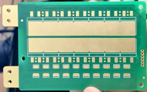
ENIG Thickness, Electroless Nickel Immersion Gold (ENIG) is one of the most widely used PCB surface finishes, providing excellent corrosion resistance, solderability, and durability. It consists of a nickel layer, which acts as a barrier and soldering surface, and a thin layer of gold, which protects the nickel from oxidation.
The thickness of the ENIG finish is crucial to ensuring reliable soldering, electrical performance, and longevity in various applications, including consumer electronics, automotive PCBs, medical devices, and aerospace systems. Understanding ENIG thickness specifications and its impact on PCB functionality is essential for manufacturers and designers.

ENIG Thickness
2. Standard ENIG Thickness Requirements
The ENIG finish consists of two key layers:
- Nickel Layer – Provides mechanical strength and acts as a diffusion barrier.
- Gold Layer – Prevents oxidation and ensures solderability.
1. Typical Thickness Range
- Nickel Layer: 3 to 6 μm (118 to 236 μin)
- Gold Layer: 0.05 to 0.23 μm (2 to 9 μin)
The gold layer in ENIG is extremely thin, as it primarily serves a protective role rather than a conductive one. The nickel layer plays a more critical role in solder joint formation and mechanical integrity.
2. Industry Standards for ENIG Thickness
ENIG thickness requirements are defined by international PCB standards, such as:
- IPC-4552A (Standard for ENIG finish)
- Gold: 0.05 – 0.23 μm (2 – 9 μin)
- Nickel: 3 – 6 μm (118 – 236 μin)
- ISO and JEDEC Standards also provide guidelines for ENIG layer consistency.
3. Impact of ENIG Thickness on PCB Performance
1. Solderability and Reliability
- If the gold layer is too thin, oxidation of the nickel layer can occur, leading to poor solderability.
- If the gold layer is too thick, excessive gold can cause “gold embrittlement,” leading to brittle solder joints.
- The nickel thickness ensures mechanical strength, preventing pad lift and cracking during assembly.
2. Electrical Performance
- Nickel thickness affects impedance control, making it crucial for RF and high-frequency PCBs.
- Gold ensures low contact resistance, improving performance in high-reliability applications like aerospace and medical electronics.
3. Prevention of Black Pad Defect
- Black pad is a common ENIG failure issue, caused by excessive nickel corrosion during the gold immersion process.
- Proper nickel thickness (≥ 3 μm) and controlled gold deposition help prevent this defect.
4. Applications of Different ENIG Thicknesses
Different industries require specific ENIG thickness levels based on soldering needs, durability, and electrical performance:
- Standard Consumer Electronics: Nickel: 3-5 μm, Gold: 0.05-0.15 μm
- Automotive and Aerospace PCBs: Nickel: 4-6 μm, Gold: 0.1-0.2 μm
- High-Frequency PCBs (RF & 5G): Nickel: 3-5 μm, Gold: 0.1-0.23 μm
- Gold Wire Bonding PCBs: Requires thicker gold (~0.2-0.3 μm) for strong bonding reliability
5. Challenges in ENIG Thickness Control
Despite its advantages, controlling ENIG layer thickness presents several challenges:
1. Gold Thickness Variability
- Gold thickness can vary across different PCB areas, affecting solder joint reliability.
- Manufacturers use tight process controls and bath chemistry adjustments to maintain uniformity.
2. Nickel Surface Roughness
- Inconsistent nickel plating thickness can lead to poor gold adhesion and defects.
- Chemical process optimization ensures smooth and uniform nickel deposition.
3. Cost Considerations
- Gold is an expensive material, and thicker gold layers increase PCB manufacturing costs.
- Engineers must balance cost vs. performance by selecting the optimal gold thickness for the application.
6. Alternative Surface Finishes Compared to ENIG
If ENIG thickness control becomes a challenge, alternative finishes may be considered:
- ENEPIG (Electroless Nickel Electroless Palladium Immersion Gold): More resistant to black pad defects.
- HASL (Hot Air Solder Leveling): A lower-cost but less precise option.
- OSP (Organic Solderability Preservative): A cost-effective, lead-free finish for basic PCB applications.
Each surface finish has its advantages and trade-offs, but ENIG remains one of the best options for high-reliability applications.
7. Conclusion
ENIG thickness plays a crucial role in PCB performance, solderability, and longevity. The nickel layer ensures mechanical strength, while the gold layer protects against oxidation. Maintaining the correct ENIG thickness is essential for preventing black pad defects, optimizing soldering performance, and ensuring long-term reliability.
For precision-controlled ENIG PCB manufacturing, Shuoqiang Electronics provides high-quality surface finishes with strict thickness control to meet IPC-4552A and industry standards. Contact us today for custom ENIG PCB solutions!
- long board pcb
- Flexible PCBs
- Special PCB
- Express Printed Circuit Board
- Pcb Prototype
- LED PCB
- PCB
- Printed Circuit Board
- Pcb meaning
- Pcb manufacturer
- Rigid pcb board
- Rigid Flex PCB

 Quote
Quote
 E-mail