The electronics industry is advancing at lightning speed, with devices shrinking in size while their power surges ahead. You’re faced with a critical decision: HDI PCB or Traditional PCB? What separates these two seemingly similar options, and how do you know which one fits your project?
The answer isn’t just in the cost or complexity—it’s in the design, the performance, and the future-proofing of your technology.
Let’s pull back the curtain and reveal what truly sets HDI PCBs apart from their traditional counterparts.
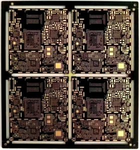
HDI PCB
HDI PCB: Redefining Innovation in Circuit Design
High-Density Interconnect (HDI): A Masterpiece of Modern Engineering
Imagine a circuit board that holds more components than ever before, but is half the size. HDI PCBs use state-of-the-art technology, incorporating microvias, blind vias, and buried vias to maximize real estate. The result? A marvel of compact efficiency.
Here’s what makes HDI shine:
- Microvias: Tiny holes, often less than 0.15mm, that connect layers with precision.
- Increased Layer Density: Pack more functionality into a smaller space.
- Improved Signal Integrity: Reduced signal loss, even in high-speed applications.
From smartphones to medical devices, HDI PCBs drive innovation where space and performance are at a premium.
Traditional PCB: Reliable, Simple, and Cost-Effective
The Workhorse of Electronics
Traditional PCBs are the backbone of countless devices, providing simplicity and reliability for basic electronic needs. Using through-hole vias and fewer layers, these boards are straightforward to manufacture and perfect for projects that don’t demand advanced capabilities.
Why traditional still holds value:
- Cost-Effectiveness: Ideal for high-volume production with low complexity.
- Ease of Manufacturing: Streamlined production processes.
- Durability: Solid for larger components and basic electronics.
Think household appliances, LED lighting, or simple control systems. Traditional PCBs get the job done, without the bells and whistles.
What’s the Real Difference Between HDI PCB and Traditional PCB?
It’s in the Details.
Design and Structure
HDI PCBs are like skyscrapers—layer upon layer of functionality packed into a confined space. Traditional PCBs, on the other hand, are more like suburban homes: spacious, reliable, but not built for vertical expansion.
HDI boards use:
- Microvias to create direct, efficient connections.
- Stacked or staggered vias for enhanced layer interconnectivity.
Traditional PCBs rely on:
- Through-hole vias, which are less space-efficient.
- Fewer layers, making them less suited for compact designs.
Performance and Application
HDI PCBs are the champions of speed and efficiency. Their reduced electrical paths lead to higher signal integrity, making them perfect for high-speed circuits in smartphones, aerospace, and medical technologies.
Traditional PCBs, with their simpler design, excel in applications where high-speed performance isn’t necessary. Think about basic gadgets like remotes or kitchen appliances.
Manufacturing Complexity
Producing HDI PCBs requires advanced techniques, like laser drilling for microvias and precise lamination for multiple layers. Traditional PCBs are far less complex, utilizing standard drilling and assembly processes.
When to Choose HDI PCB Over Traditional PCB
Think Miniaturization and Complexity
If your device demands:
- Compact size with high functionality
- High-speed performance
- Advanced reliability in harsh environments
Then HDI PCB is your go-to solution.
On the other hand, if your project is:
- Cost-sensitive and straightforward
- Built for larger, less dense circuits
- Focused on durability without complexity
Traditional PCBs are a better fit.
The Future of PCB Technology
The demand for HDI PCBs is skyrocketing. As devices become smarter, smaller, and faster, manufacturers are pushing the boundaries of HDI capabilities. At the same time, innovations in traditional PCB manufacturing continue, making them more efficient and eco-friendly.
The real winner here? The industry—and the consumers who benefit from cutting-edge devices built on the right technology.
Make the Right Choice for Your Project
Your decision between HDI PCB and Traditional PCB isn’t just about specs. It’s about the future of your product. Choose wisely, and you’ll deliver a solution that’s not only functional but groundbreaking.
Ready to take the next step? Explore the possibilities of HDI and Traditional PCBs with experts who can guide your project to success.
our linken sqpcb.com

- long board pcb
- Flexible PCBs
- Special PCB
- Express Printed Circuit Board
- Pcb Prototype
- LED PCB
- PCB
- Printed Circuit Board
- Pcb meaning
- Pcb manufacturer
- Rigid pcb board
- Rigid Flex PCB
 Quote
Quote
 E-mail