PCB Board Meaning: Take a moment to think about the devices you use every day—your smartphone, laptop, or even the dashboard of your car. Sleek, fast, and powerful, they’re marvels of modern engineering. But here’s the truth: none of them would function without one key component hidden beneath the surface.
The PCB board.
This silent workhorse is the foundation of every electronic device. It’s not flashy or glamorous, but it’s indispensable. Without it, your devices wouldn’t just stop working—they wouldn’t exist.
But what exactly is a PCB meaning in electronics? What makes it the backbone of modern technology? To answer these questions, let’s start from the ground up.
pcb board meaning
What Is a PCB Board, PCB Board Meaning?
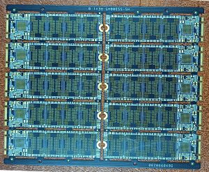
The term “PCB” stands for Printed Circuit Board. Think of it as a meticulously crafted roadmap for electricity. Each copper trace, each layer, and every component is designed to ensure seamless communication between the electronic parts of a device.
Unlike the tangled mess of wires used in early electronics, PCBs are clean, efficient, and incredibly reliable. They provide structure and connectivity, allowing electrical signals to flow with precision. Whether it’s a single-sided PCB for simple gadgets or a multilayer PCB used in advanced technologies, these circuit boards are the foundation of modern electronics.
The Anatomy of a PCB Board
Every PCB board is a masterpiece of design, made up of several critical layers:
- Substrate: The base material, usually fiberglass (FR-4), provides mechanical support and durability.
- Copper Layer: Conductive pathways etched to create circuits, enabling the flow of electricity.
- Solder Mask: A protective layer that prevents oxidation and accidental shorts while giving the board its characteristic color.
- Silkscreen: The labeling layer that helps identify PCB components and their placement during PCB assembly.
These elements combine to create a sturdy, reliable platform for powering devices across industries.
Types of PCB Boards and Their Uses
PCB boards are not one-size-fits-all. Depending on the application, they come in different types:
- Single-Sided PCB: Simple and cost-effective, ideal for low-complexity devices like calculators.
- Double-Sided PCB: A step up, used in applications like LED lighting and small appliances.
- Multilayer PCB: Found in smartphones, computers, and advanced industrial equipment, offering enhanced functionality.
- Flexible PCB: Perfect for devices requiring bendable circuit boards, such as wearable technology.
- Rigid PCB: Common in consumer electronics due to their durability and stability.
- Rigid-Flex PCB: A hybrid design that combines the best of rigid and flexible PCBs for compact and versatile applications.
Each type of PCB design is tailored to meet specific performance needs, proving that PCBs are as versatile as they are essential.
Why Are PCB Boards So Important?
From consumer gadgets to life-saving medical devices, PCB boards are everywhere. They ensure reliability, compactness, and efficiency in electronic systems. Without printed circuit boards, the devices we rely on would be bulkier, less efficient, and prone to failure.
They are not just components; they are enablers of innovation. They allow engineers to design smaller, faster, and more powerful devices that push the boundaries of what’s possible.
How PCB Boards Are Made
Creating a PCB board is a precise and detailed process that combines engineering, craftsmanship, and quality control to deliver a reliable product. Here’s a deeper look at each step:
1. Design
- Engineers begin by designing the blueprint of the PCB using specialized software like Altium Designer, KiCad, or EasyEDA.
- The design process includes creating the PCB layout, defining the copper traces, and specifying the placement of components.
- Signal integrity analysis and thermal management considerations are incorporated to ensure high performance.
- Design rules are checked to prevent issues during manufacturing, such as spacing violations or overlapping traces.
2. Fabrication
- The process starts with the substrate, commonly FR-4, which is chosen for its durability and cost-effectiveness.
- A copper layer is applied, and a photolithography process transfers the circuit design onto the board.
- Unwanted copper is etched away, leaving only the desired circuit pathways.
- For multilayer PCBs, layers are stacked and laminated under high pressure and temperature to form a single cohesive board.
- Drill holes and vias are created to connect different layers and provide pathways for electrical signals.
3. Testing and Quality Control
- Rigorous testing is conducted to ensure the PCB meets design specifications and functions as intended:
- Automated Optical Inspection (AOI): Cameras scan the board for defects such as misaligned components or broken traces.
- Electrical Testing: Continuity tests verify the integrity of the circuit pathways.
- Functional Testing: The assembled board is tested in a simulated environment to ensure proper operation.
- Advanced techniques like X-ray inspection may be used for multilayer PCBs to check hidden solder joints or internal connections.
4. Surface Finishing
- A surface finish is applied to protect the exposed copper and improve solderability. Common finishes include HASL, ENIG, and OSP, selected based on the application and budget.
5. Final Inspection and Packaging
- The completed PCB undergoes a final visual inspection to check for any remaining defects.
- Boards are cleaned to remove flux residues and packaged to protect them during shipping.
- Serial numbers or QR codes may be added for traceability and inventory management.
This process, though intricate, ensures that each PCB is ready to handle the demands of its intended application.
Future Trends in PCB Technology
The world of PCBs is constantly evolving. As devices become smaller and more powerful, PCB boards must adapt. Emerging trends include:
- Miniaturization: High-density interconnect (HDI) technology is enabling even smaller and more efficient multilayer PCBs.
- Eco-Friendly Materials: The industry is exploring recyclable and biodegradable materials to reduce environmental impact.
- 3D Printing: Rapid prototyping and cost-effective production are becoming more accessible for printed circuit boards.
These advancements are shaping the future of electronics, making PCB boards more essential than ever.
Conclusion
The meaning of PCB board is more than just a piece of hardware. It’s the backbone of modern technology, enabling the devices that power our lives. By understanding its meaning, components, and significance, you gain insight into the engine behind innovation.
Whether you’re a tech enthusiast, a professional, or simply curious, the world of PCB boards is one worth exploring. Every great invention begins with a solid foundation—and for electronics, that foundation is the PCB board.
linkedin sqpcb.com
https://lnkd.in/gCut3MrT

- long board pcb
- Flexible PCBs
- Special PCB
- Express Printed Circuit Board
- Pcb Prototype
- LED PCB
- PCB
- Printed Circuit Board
- Pcb meaning
- Pcb manufacturer
- Rigid pcb board
- Rigid Flex PCB
 Quote
Quote
 E-mail