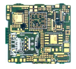
Pcb fabrication:Printed Circuit Boards (PCBs) form the backbone of modern electronics, connecting components in a compact, organized, and functional layout. Whether for hobbyists or professionals, PCB fabrication demands precision, patience, and a methodical approach. This guide provides a detailed walkthrough of the printed circuit board fabrication process, from design to final assembly.
Pcb fabrication
Step 1: Design the PCB Layout
The first and most crucial step in PCB fabrication is designing the PCB layout using software like Eagle, KiCad, or Altium Designer.
- Component Placement: Arrange components logically to minimize trace lengths and reduce interference.
- Layer Configuration: For complex circuits, opt for multi-layer PCBs to accommodate intricate designs.
- Finalize Design: Perform a Design Rule Check (DRC) to ensure all elements meet specifications and export Gerber files for PCB board fabrication.
Step 2: Print the PCB Design
Convert the finalized design into a transferable format.
- Print the Layout: Use a laser printer to create a mirrored image of the PCB design on glossy paper. This step is critical for single-sided and double-sided printed circuit board fabrication.
- Professional Methods: Use photomasks and UV-sensitive boards for precise and professional results, commonly employed in advanced PCB prototype fabrication services.
Step 3: Prepare the PCB Board
Start with a copper-coated PCB substrate.
- Cut and Clean: Trim the board to size and clean its surface with fine sandpaper to remove oxidation, a vital step in PCB board fabrication.
- Mark Layer Sides: For double-sided boards, label each layer to ensure proper alignment.
Step 4: Transfer the Design to the PCB
Choose between the toner transfer or photoresist method to imprint the design onto the copper surface.
- Toner Transfer Method: Apply heat to transfer toner from the paper to the PCB, a common practice in small-scale PCB prototype fabrication services.
- Photoresist Method: Expose the board to UV light to develop the resist pattern, ideal for precision in printed circuit board fabrication.
Step 5: Etch the PCB
Remove unwanted copper to reveal the designed traces.
- Prepare the Etchant: Use ferric chloride or a hydrochloric acid solution, essential materials for successful PCB fabrication.
- Etching Process: Submerge the PCB in the etchant, agitating gently until the design is visible.
- Rinse and Dry: Wash off the etchant and dry the board thoroughly to finalize this stage of PCB board fabrication.
Step 6: Drill the PCB
Drill holes for through-hole components and vias.
- Precision Tools: Use carbide bits and a drill press for clean and accurate holes, ensuring they meet the standards for professional printed circuit board fabrication.
- Alignment: Ensure holes match the component placement on the layout.
Step 7: Apply the Solder Mask (Optional)
Protect copper traces and enhance durability with a solder mask.
- Solder Mask Application: Apply the mask and cure it with UV light. This step elevates the quality of PCB prototype fabrication services.
- Peel Excess: Remove the excess mask, leaving solder pads exposed.
Step 8: Apply the Silkscreen (Optional)
Add labels and component identifiers for assembly and troubleshooting.
- Silkscreen Application: Use white ink or markers for DIY boards, or opt for professional silkscreen machines for printed circuit board fabrication.
- Ensure Legibility: Clear markings simplify assembly and future repairs.
Step 9: Solder Components onto the PCB
Populate the board with components as per the schematic.
- Organize Components: Begin with smaller parts and progress to larger ones.
- Soldering Tips: Use minimal solder for secure, clean connections, avoiding overheating sensitive components.
- Inspection: Check for cold solder joints or bridges between pads, ensuring compliance with PCB board fabrication standards.
Step 10: Test the PCB
Verify the functionality of the completed board.
- Basic Tests: Conduct continuity tests to ensure connections are correct.
- Functional Testing: Apply power and test each section according to the design. Testing is a crucial phase in PCB prototype fabrication services to ensure quality.
- Troubleshooting: Address any shorts, incorrect connections, or assembly errors.
Conclusion
PCB fabrication is a rewarding process that transforms a concept into a tangible, functional circuit board. Whether for a prototype or a final product, following these steps ensures precision and reliability. With the right tools and the support of professional PCB prototype fabrication services, you can master printed circuit board fabrication and bring your electronic designs to life.

- long board pcb
- Flexible PCBs
- Special PCB
- Express Printed Circuit Board
- Pcb Prototype
- LED PCB
- PCB
- Printed Circuit Board
- Pcb meaning
- Pcb manufacturer
- Rigid pcb board
- Rigid Flex PCB
 Quote
Quote
 E-mail