The demand for custom PCB manufacturing is growing across industries, from electronics and medical devices to automotive and telecommunications. Customized PCB manufacturing is a specialized process that transforms unique design requirements into functional, high-quality circuit boards. Understanding each step involved in PCB manufacturing can help clients and engineers make informed decisions and achieve optimal results. This article breaks down the essential steps in custom PCB manufacturing, highlighting the careful coordination and precision needed at each phase.
custom PCB manufacturing
Custom PCB manufacturing Step 1: PCB Design and Layout
The first and perhaps most critical step in customized PCB manufacturing is the design phase. During this stage, engineers use specialized software (such as Altium Designer, Eagle, or KiCAD) to create the PCB board layout based on the product’s functional and performance requirements. This layout includes the placement of components, connections, layers, and routing paths that allow the circuit to function as intended. Designers must also consider factors like signal integrity, thermal management, and power distribution while ensuring that the PCB dimensions and specifications meet the end product’s constraints.
Key considerations:
- Component placement and density
- Number of layers (single, double-sided, or multi-layer)
- Signal paths and power/ground plane allocation
- Design for manufacturability (DFM) to minimize production issues
Custom PCB manufacturing Step 2: Design Verification and Prototype Testing
Before moving to full production, it’s essential to verify the PCB design to prevent costly errors. Design rule checks (DRC) are conducted to ensure that the design adheres to manufacturing guidelines, including spacing, width, and other technical requirements. Additionally, simulation tools may be used to test the electrical behavior of the circuit design.
Once verified, a prototype is created to test the PCB’s functionality in real-world conditions. Prototype testing allows engineers to evaluate the board’s performance, identify potential issues, and make necessary adjustments.
Key considerations:
- Design rule verification
- Signal simulation and integrity testing
- Thermal performance checks
- Physical prototype testing for functionality and durability
Step 3: Material Selection and Sourcing
The materials used in PCB manufacturing directly impact the board’s performance and durability. Depending on the requirements, substrate materials like FR4 (a common fiberglass epoxy laminate), polyimide, or metal-core boards may be chosen. The type of copper, solder mask, and surface finish also play an essential role in the board’s performance and lifespan. For high-frequency or high-temperature applications, advanced materials such as Rogers laminates may be preferred.
Key considerations:
- Substrate choice based on thermal, electrical, and environmental requirements
- Copper thickness for current handling and heat dissipation
- Solder mask and surface finish selection for protection and reliability
Step 4: PCB Fabrication
During fabrication, the PCB undergoes a series of processes to transform the design into a physical board. The fabrication process includes etching, laminating, and layering, where conductive copper layers are printed onto the board, creating the circuit paths. Each layer is precisely etched to match the design layout, and multiple layers are laminated together if required.
The fabrication process also includes drilling to create holes for components, vias, and interconnections, followed by plating to provide electrical connectivity between layers. Solder masking and silkscreen printing are applied as protective coatings and labels, respectively.
Key steps:
- Photolithography and etching for circuit patterning
- Lamination for multi-layer boards
- Drilling and plating for component holes and vias
- Solder mask application and silkscreen labeling
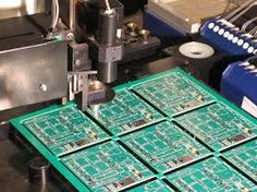
Step 5: Component Sourcing and Assembly
After the board itself is manufactured, the next phase is component sourcing and assembly. Components specified in the design (such as resistors, capacitors, and integrated circuits) are sourced from reliable suppliers to ensure quality and compatibility. During assembly, components are placed on the board according to the design layout using either Surface Mount Technology (SMT) or Through-Hole Technology (THT).
In SMT, components are placed directly on the board’s surface, making it ideal for compact and complex designs. THT, on the other hand, involves inserting component leads through drilled holes and is often used for components requiring mechanical stability.
Key considerations:
- Ensuring component compatibility and quality
- Deciding on assembly technology (SMT or THT)
- Proper alignment and soldering to prevent defects
Step 6: Quality Control and Testing
Quality control (QC) is a vital part of customized PCB manufacturing. After assembly, each PCB undergoes rigorous testing to ensure it meets all specifications and functions as intended. Automated Optical Inspection (AOI) and X-ray inspection help detect issues like misaligned components, poor soldering, or hidden defects within multi-layer boards. In-Circuit Testing (ICT) and Functional Testing (FCT) are also used to validate the electrical performance of the assembled PCB.
QC processes are essential in detecting issues early and ensuring that only high-quality boards reach the client.
Key tests:
- AOI and X-ray inspection for physical defects
- ICT and FCT for electrical testing
- Environmental testing for boards designed to withstand extreme conditions
Step 7: Final Assembly and Packaging
Once the boards pass QC testing, they are ready for final assembly and packaging. This step may involve mounting the PCB into an enclosure or integrating it with other parts of the device. Finally, the assembled products are carefully packaged to prevent damage during transit and storage.
Depending on the client’s requirements, the PCBs may be delivered in antistatic packaging to protect against electrostatic discharge (ESD) or customized packaging for branding purposes.
Step 8: Documentation and Support
Customized PCB manufacturing doesn’t end with delivery. Clients may receive technical documentation detailing the PCB’s design, material specifications, and assembly instructions to assist with installation or further integration. Many manufacturers also offer post-delivery support, helping clients troubleshoot issues or make design adjustments for future orders.
Conclusion
Customized PCB manufacturing involves a series of precise, coordinated steps, from initial design to final quality checks. Each stage requires specialized skills, tools, and attention to detail to ensure the PCB functions as expected and meets the client’s specifications. By understanding the key steps in custom PCB manufacturing, clients and engineers can better collaborate to create reliable, high-performance boards tailored to specific applications.
our linken sqpcb.com

- long board pcb
- Flexible PCBs
- Special PCB
- Express Printed Circuit Board
- Pcb Prototype
- LED PCB
- PCB
- Printed Circuit Board
- Pcb meaning
- Pcb manufacturer
- Rigid pcb board
- Rigid Flex PCB
 Quote
Quote
 E-mail