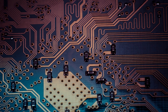
Printed Circuit Boards (PCBs) are the foundation of modern electronics, providing a platform to connect electronic components and enable their functionality in devices ranging from smartphones to industrial machinery. The fabrication of a PCB is a precise, multi-step process that transforms raw materials into complex, functional boards. This article explores each stage of the PCB fabrication process, providing a comprehensive introduction to how these essential components are made.
1. Designing the PCB Layout
The fabrication process begins with the PCB layout design. Engineers use Computer-Aided Design (CAD) software to design the board, defining the component placements, trace pathways, and via locations. The design is critical as it ensures the board functions as intended while minimizing issues such as signal interference and noise. Once the layout is finalized, it’s converted into industry-standard files, typically in Gerber format, which serve as the blueprint for the fabrication.
2. Printing the Design on Film
The PCB design is then transferred onto a film in a photoplotter machine. The machine prints a photomask of the board’s layers onto transparent films, each showing the copper trace pattern. These films provide a precise representation of the board’s layout, with black ink representing the copper areas to remain on the board and clear sections representing areas to be etched away.
3. Preparing the PCB Substrate
The substrate forms the base material of the PCB, typically made of fiberglass, epoxy, or phenolic resin. It provides the mechanical support needed to hold components in place. A thin layer of copper is laminated onto both sides of the substrate to serve as the conductive material. The thickness of the copper layer varies depending on the PCB’s intended application.
4. Transferring the Image and Etching
With the substrate prepared, the design is transferred onto the copper layer. This is done using a photoresist material—a light-sensitive film that’s applied to the copper layer. When exposed to UV light through the photomask, the photoresist hardens, protecting the copper beneath it. The board is then washed, removing the unexposed areas, and an etching solution is applied to dissolve the exposed copper, leaving only the copper traces defined by the photoresist.
5. Layer Alignment and Bonding
For multilayer PCBs, the next step is to align and bond each layer precisely. After etching, individual layers are stacked and aligned using optical devices. The layers are then pressed together under high heat and pressure to bond the materials, creating a single, unified board with the desired number of layers.
6. Drilling the Holes
Drilling holes is essential for creating vias, which electrically connect different layers of the PCB, and for placing component leads. High-precision drilling tools, often guided by CNC machines, drill tiny holes as small as 0.1mm in diameter. Once drilled, the holes are electroplated with copper to create conductive paths that link the layers and components.
7. Plating and Copper Deposition
The copper plating process ensures that all drilled holes and surface areas are conductive. In this step, the board is submerged in a chemical bath, where a thin layer of copper is deposited onto the drilled holes’ walls and over the surface of the board, connecting multiple layers and establishing continuity across the PCB.
8. Solder Mask Application
The solder mask, typically green but available in other colors, is applied to insulate the PCB surface and prevent solder bridges from forming between closely spaced components. The solder mask is applied over the entire board except for pads and holes that will be used for soldering. After application, the board undergoes a curing process to harden the mask.
9. Surface Finishing
Surface finishing is an essential process that enhances the solderability and longevity of the board. Common finishes include HASL (Hot Air Solder Leveling), ENIG (Electroless Nickel Immersion Gold), and OSP (Organic Solderability Preservative). These finishes prevent oxidation and improve the adhesion of components during assembly.
10. Silkscreen Printing
The silkscreen layer is printed onto the board, adding essential markings such as component labels, logos, and other identifiers. This layer is usually applied in white or black ink and helps assembly technicians and repair professionals easily identify components on the PCB.
11. Electrical Testing
Before a PCB is ready for use, it undergoes a series of electrical tests to ensure functionality and continuity across all traces. Testing methods include the flying probe test, where probes touch different points on the PCB to verify the circuit, and the bed-of-nails test for large-scale productions. This step identifies any defects, shorts, or open circuits that may have occurred during fabrication.
12. Cutting and Final Inspection
After testing, the PCB panels are cut into individual boards using routers or v-scorers. A final inspection is performed to ensure there are no visual defects, such as misaligned layers or incomplete finishes. Each PCB is examined to verify it meets quality standards before moving to the next phase of assembly or shipping.
Conclusion
The PCB fabrication process is a meticulous journey from design to the final product, involving multiple steps to ensure accuracy, durability, and performance. As technology continues to evolve, advances in PCB fabrication techniques promise even greater precision, efficiency, and adaptability, supporting the growth of the electronics industry. Understanding this process offers insight into the complex groundwork that powers our most essential devices.

- long board pcb
- Flexible PCBs
- Special PCB
- Express Printed Circuit Board
- Pcb Prototype
- LED PCB
- PCB
- Printed Circuit Board
- Pcb meaning
- Pcb manufacturer
- Rigid pcb board
- Rigid Flex PCB
 Quote
Quote
 E-mail