The Essential Guide to PCB Boards Manufacturing: Key Steps Explained
- Introduction
- 1. PCB Boards Manufacturing: Cutting the Raw Material
- 2. PCB Boards Manufacturing: Inner Layer Processing
- 3. Lamination and Pressing
- 4. Drilling Process
- 5. Electroplating Process
- 6. Outer Layer Processing
- 7. Solder Mask Application
- 8. Text and Legend Printing
- 9. Surface Finishing
- Conclusion
- Frequently Asked Questions (FAQ)
Introduction
Printed Circuit Boards (PCBs) are fundamental components in modern electronics, providing a structural and electrical foundation for connecting and supporting electronic components. The PCB manufacturing process is intricate and involves a series of highly precise steps, ensuring optimal functionality, reliability, and durability. This guide outlines the key stages in PCB manufacturing, highlighting the critical steps and considerations involved in creating high-quality PCBs.

whats pcb manufacturing process
1. PCB Boards Manufacturing: Cutting the Raw Material
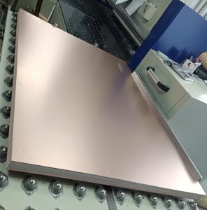
The manufacturing process begins with cutting the raw PCB material. The material, typically fiberglass-reinforced copper foil, is cut to the required size. The accuracy of cutting is critical, with a tolerance of +/-2mm. Common material sheet sizes include 36”*48”, 40”*48”, and 42”*48”. Material utilization is important for reducing waste, and in special cases, materials can be mixed for cutting to optimize production efficiency.
2. PCB Boards Manufacturing: Inner Layer Processing
This stage involves several sub-processes:
Pre-treatment: Cleaning and preparing the laminate to ensure a contaminant-free surface.
Coating: Applying a photosensitive coating on the laminate surface.
Exposure: Using a photomask to expose the coating to UV light, transferring the design pattern onto the laminate.
Development and Etching: Developing the exposed pattern and removing unwanted copper using a chemical etching solution.
Drilling: Drilling holes for vias and component leads.
AOI (Automated Optical Inspection): Conducting visual inspection to ensure quality.
At SQPCB, advanced techniques such as LDI (Laser Direct Imaging) exposure machines and fully automated coating and baking lines are used. The use of LDI technology minimizes film shrinkage issues, ensuring precise alignment and reducing registration errors. This innovation helps maintain controlled shrinkage within 0.1um, improving the overall quality of the inner layers.
Inner Layer Ink Pre-Baking
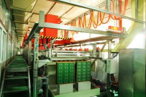
3. Lamination and Pressing
The lamination process involves the bonding of multiple layers to create multi-layer PCBs. This step includes:
Brown-Out and Riveting: Pre-pressing the laminate to form a stable base.
Pre-Stacking: Aligning the stacked layers of copper, laminate, and prepregs.
Pressing: Applying heat and pressure to bond the layers together.
X-ray Drilling Targets: Drilling targets are aligned and inspected using X-ray systems.
Edge Trimming and Grinding: Trimming the edges and ensuring uniformity in thickness.
Pressing is one of the most critical steps in multi-layer PCB production. SQPCB has optimized this process by selecting structures that not only meet the required board thickness but also improve impedance control. Materials such as 7628 are selected over more expensive options like 2116, significantly reducing costs while ensuring high performance.
PCB Laminating Machines
4. Drilling Process
Drilling is a crucial step for creating holes for vias and through-hole components. It involves:
Pre-Drilling: Initial drilling to prepare the material for deeper cuts.
Drill Bit Grinding: Ensuring the drill bits are sharpened to maintain precision.
Pinning and Drilling: Ensuring accurate hole placement and depth.
Drill Bit Retirement and Peak Polishing: Polishing drill bits after 3,000-5,000 holes to maintain their effectiveness.
SQPCB uses linear motor-driven drilling machines, ensuring high-speed and high-precision drilling. These machines guarantee hole accuracy and consistency, ensuring that all holes meet IPC standards with a tolerance of +/-2mil.
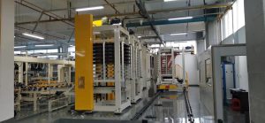
5. Electroplating Process
Electroplating is essential for copper deposition inside drilled holes and on the PCB surface. The process includes:
High-pressure Water Washing: Ensuring the board is clean before electroplating.
PTH (Plated Through-Hole): Plating copper inside the holes for electrical conductivity.
Copper Electroplating: Depositing a thin layer of copper onto the surface and inside the holes to ensure good electrical connections.
SQPCB uses renowned electroplating equipment, investing in high-quality systems that improve yield and reduce the failure rate. While equipment costs may be higher, the long-term benefits of reduced downtime and superior quality outweigh the initial investment.
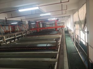
PCB Copper Electroplating Lines
6. Outer Layer Processing
After the inner layers are completed, the outer layer processing begins. It includes:
Pre-treatment: Cleaning the copper surface before applying the protective coatings.
Film Lamination: Applying a protective film for further processing.
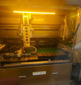
Exposure and Development: Using LDI technology to transfer the design onto the outer layer.
Etching and Removal: Removing the unwanted copper, leaving behind the designed circuit pattern.
AOI and Impedance Testing: Ensuring the design meets the required impedance and quality standards.
At SQPCB, LDI exposure machines with linear motor and optical scale control help achieve shrinkage accuracy within 0.1um, ensuring excellent alignment and reducing defects caused by manual handling.

LDI exposurer
7. Solder Mask Application
A solder mask is applied to the PCB to protect copper traces and prevent solder bridges during the assembly process. The steps include:
Pre-treatment and Silk Printing: Printing the solder mask onto the PCB.
Pre-baking: Pre-curing the solder mask to harden it before exposure.
Exposure and Development: Using UV light to expose and harden the mask where needed.
SQPCB implements automated solder mask applications, significantly reducing manual errors such as solder mask shift or incorrect pad coverage. This system helps maintain uniformity and ensures a high-quality finish for all PCBs.
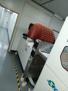
8. Text and Legend Printing
Text and legends are applied to the PCB to mark components, references, and other essential information. The process includes:
Silk Screen and Inkjet Printing: Printing labels and other markings.
Post-Baking: Curing the printed ink to ensure durability.
SQPCB uses linear motor-driven inkjet printing machines, achieving exceptional control over shrinkage and print accuracy. This technology reduces defects caused by misalignment and guarantees clear, legible text.

Legend printer
9. Surface Finishing
A surface finish is applied to exposed copper areas to protect against oxidation and improve solderability. This step includes:
Gold Immersion (ENIG), HASL, or OSP: The choice of surface finish is based on customer requirements for durability and solderability.
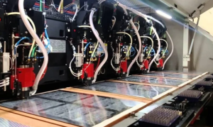
10. Final Inspection and Electrical Testing
Before assembly, PCBs undergo a series of tests to ensure their functionality:
Electrical Testing: Detects open circuits, short circuits, or misalignments.
Flying Probe Testing and AOI: Ensure the PCB meets design specifications.
Final inspection is essential to ensure that no defects are present and the PCBs meet industry standards before packaging.
Flying Probe Test
Conclusion
PCB manufacturing is a detailed and complex process that requires precision and careful attention to detail at each stage. From the initial design to final inspection, every step plays a critical role in ensuring the PCB’s functionality, reliability, and durability. SQPCB provides cutting-edge technology and processes at every stage of production, ensuring that your PCBs are produced to the highest standards of quality and precision.
By following this comprehensive guide and collaborating with experts like SQPCB, businesses can achieve optimal results in express PCB manufacturing, delivering high-quality products that meet stringent performance requirements.
Frequently Asked Questions (FAQ)
What is the first step in the PCB manufacturing process?
The first step is the design and schematic capture, where engineers define all the electrical connections and component placements using specialized software.
Why is etching important in PCB manufacturing?
Etching is used to remove unwanted copper from the PCB, leaving behind the precise copper traces required for the PCB’s circuit pathways.
How does SQPCB ensure high-quality PCB production?
SQPCB employs advanced equipment, such as LDI exposure machines and linear motor-driven drilling systems, to achieve precise alignment and improve manufacturing accuracy.
What are some common surface finishes for PCBs?
Common surface finishes include HASL, ENIG (Electroless Nickel Immersion Gold), and OSP, each offering different levels of solderability and protection against oxidation.
What types of tests are performed on PCBs before assembly?
Electrical tests, AOI, and flying probe testing are used to verify that the PCB is free of defects such as short circuits or misalignments, ensuring reliable performance.

- long board pcb
- Flexible PCBs
- Special PCB
- Express Printed Circuit Board
- Pcb Prototype
- LED PCB
- PCB
- Printed Circuit Board
- Pcb meaning
- Pcb manufacturer
- Rigid pcb board
- Rigid Flex PCB
 Quote
Quote
 E-mail