22 Layer PCB & High-Layer Circuit Boards: Design, Manufacturing, and Applications
Introduction
As modern electronics become more complex, high-layer circuit boards play a crucial role in supporting high-speed, high-frequency, and high-density electronic applications. A 22-layer PCB is a multi-layer printed circuit board (PCB) designed to handle advanced signal integrity, power distribution, and thermal management requirements. These boards are widely used in aerospace, telecommunications, high-performance computing, and medical electronics, where reliability and performance are critical.
This article explores the structure, design considerations, manufacturing process, advantages, and key applications of 22-layer PCBs and high-layer circuit boards.
22 layer pcb
What is a 22-Layer PCB?
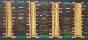
A 22-layer PCB is a high-layer circuit board consisting of 22 stacked layers of copper traces, dielectric materials, and insulating layers. These layers are laminated together to form a compact, high-density PCB capable of supporting high-speed data transmission and complex signal routing.
Key Layers in a 22-Layer PCB
A 22-layer PCB typically consists of:
- Top and Bottom Layers – Used for component mounting and primary signal routing.
- Inner Signal Layers – Dedicated layers for high-speed and low-speed signal transmission.
- Power and Ground Planes – Provide stable voltage distribution and reduce electromagnetic interference (EMI).
- Core and Prepreg Layers – Dielectric insulating materials that bond PCB layers together.
- Controlled Impedance Layers – Essential for high-frequency applications like RF, microwave, and 5G communication systems.
Why Use a 22-Layer PCB or High-Layer Circuit Board?
The main advantage of a 22-layer PCB is its ability to support complex circuits, high-speed signals, and multi-functional electronic systems.
1. Supports High-Speed Data Transmission
✔ Reduces signal loss and crosstalk, ensuring better signal integrity.
✔ Maintains impedance control, essential for 5G, AI, and HPC (High-Performance Computing) applications.
2. Increased Routing Capacity
✔ More layers allow for compact, high-density circuit designs.
✔ Supports multiple differential pairs for interfaces like PCIe, DDR5, and USB 4.0.
3. Improved Power Distribution
✔ Dedicated power and ground planes enhance power integrity.
✔ Reduces voltage fluctuations, crucial for multi-layered server and data center PCBs.
4. Advanced Thermal Management
✔ Copper planes help dissipate heat efficiently.
✔ Suitable for high-power applications, such as automotive radar, aerospace navigation, and industrial automation.
5. Enhanced EMI and Noise Control
✔ Controlled impedance layers help reduce electromagnetic interference (EMI).
✔ Ideal for high-frequency and RF circuit applications.
Manufacturing Process of a 22-Layer PCB
Producing a 22-layer PCB involves multiple high-precision steps to ensure quality, reliability, and performance.
Step 1: Material Selection
- Common substrates: FR-4, High-Tg FR-4, Rogers, Polyimide.
- Copper foil thickness: 1oz to 2oz depending on current-carrying requirements.
Step 2: Inner Layer Fabrication
- Copper layers are etched to form signal traces.
- Alignment and registration ensure accuracy for high-density interconnects.
Step 3: Lamination Process
- Prepreg (insulating material) and core layers are stacked.
- High-temperature pressing fuses the layers together to form a single board.
Step 4: Drilling and Via Formation
- Through-hole, blind, and buried vias are drilled using laser or mechanical drilling.
- Copper plating is applied to vias to establish electrical connections.
Step 5: Surface Treatment
- ENIG (Electroless Nickel Immersion Gold) is commonly used for corrosion resistance and better solderability.
- Other options include HASL (Hot Air Solder Leveling), Immersion Silver, or OSP (Organic Solderability Preservatives).
Step 6: Testing and Quality Control
- Electrical testing (E-test) ensures no short circuits or open circuits.
- X-ray inspection checks inner layers and hidden vias.
- Final functional tests validate PCB performance under real-world conditions.
Design Considerations for 22-Layer PCBs
When designing a high-layer circuit board, engineers must focus on signal integrity, power distribution, and manufacturability.
1. Controlled Impedance Design
✔ Essential for high-frequency signals and differential pairs.
✔ Ensures consistent signal propagation and minimal losses.
2. Via Selection
✔ Blind, buried, and via-in-pad techniques improve signal routing.
✔ Microvias enable high-density interconnects (HDI) for miniaturized devices.
3. Power and Ground Plane Optimization
✔ Dedicated power layers reduce noise and voltage drop.
✔ Low-impedance ground layers improve EMI shielding.
4. Signal Layer Stack-up Optimization
✔ Arranging signal and power layers in a balanced configuration ensures minimal interference.
✔ High-speed PCB designs require stripline or microstrip routing techniques.
Applications of 22-Layer PCBs and High-Layer Circuit Boards
22-layer PCBs are used in high-performance and mission-critical applications where reliability, speed, and durability are essential.
1. Telecommunications and 5G Networks
- High-frequency circuit boards for 5G base stations, optical networking, and satellite communication.
- Ensures low latency and high signal integrity.
2. Aerospace and Defense Electronics
- Used in radar systems, avionics, and satellite navigation units.
- Requires high-reliability PCB materials and strict quality control.
3. Data Centers and AI Computing
- Supports server motherboards, high-speed data interconnects, and AI accelerator boards.
- Manages large-scale data processing with minimal power loss.
4. Automotive Electronics
- Found in ADAS (Advanced Driver Assistance Systems), EV power management, and infotainment.
- Resistant to high temperatures and vibrations.
5. Medical Equipment and Imaging Systems
- Used in MRI, CT scanners, and patient monitoring devices.
- High signal accuracy ensures precise diagnostics and patient safety.
Challenges in Manufacturing 22-Layer PCBs
Despite their advantages, high-layer PCBs pose several challenges:
❌ Complex Stack-up Management – Requires precise alignment and layer control.
❌ Drilling Accuracy – Microvias and deep vias require high-precision laser drilling.
❌ Thermal Expansion Control – Different materials expand at different rates, causing stress on vias and traces.
❌ High Manufacturing Costs – More layers increase fabrication time and cost.
To overcome these challenges, experienced PCB manufacturers use advanced lamination, laser drilling, and automated quality control.
Conclusion
A 22-layer PCB is a highly sophisticated circuit board designed for complex, high-speed, and high-reliability applications. Its multi-layer architecture enables better signal integrity, efficient power distribution, and superior thermal management, making it ideal for telecommunications, aerospace, data centers, automotive, and medical electronics.
Due to design complexity and manufacturing precision, choosing a reliable PCB manufacturer is crucial for ensuring quality and performance.
At Shuoqiang Electronics, we specialize in high-layer PCB manufacturing, providing custom solutions for high-performance applications. Contact us today for your 22-layer PCB and multi-layer circuit board needs!

- long board pcb
- Flexible PCBs
- Special PCB
- Express Printed Circuit Board
- Pcb Prototype
- LED PCB
- PCB
- Printed Circuit Board
- Pcb meaning
- Pcb manufacturer
- Rigid pcb board
- Rigid Flex PCB
 Quote
Quote
 E-mail