1. Introduction to Wet Etching vs. Dry Etching in PCB Manufacturing
The field of printed circuit board (PCB) manufacturing has undergone extensive evolution over the past few decades, largely driven by the push for higher circuit densities, smaller feature sizes, and better overall performance. Among the most critical processes in the fabrication of PCBs is the etching stage, which defines the conductive pathways that interconnect various electronic components. Two primary techniques have emerged in this context: wet etching and dry etching. These methods differ significantly in terms of their mechanisms, equipment requirements, material compatibility, environmental impact, and application scope.
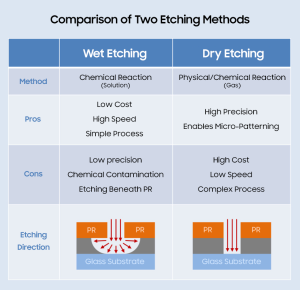
Understanding the distinctions between wet etching and dry etching is essential for engineers and manufacturers seeking to optimize production lines for specific product requirements. Wet etching typically involves the use of liquid chemicals to remove unwanted copper from PCB substrates, whereas dry etching uses gas-phase reactions, often in a plasma environment, to achieve the same objective. Both methods are capable of producing high-quality circuit patterns, but the trade-offs between cost, resolution, throughput, and ecological footprint can significantly influence the selection process.
From a broader perspective, the choice between these two approaches is emblematic of the tensions that often arise between legacy technologies and more modern innovations. Wet etching, despite being an older and more established method, remains widely used due to its relative simplicity and low operational costs. On the other hand, dry etching has gained prominence in high-end and specialized applications where precision and process control are paramount.
This comparison becomes especially pertinent as PCB designs become more complex. The advent of high-density interconnect (HDI) boards, embedded components, and advanced packaging techniques calls for a deeper understanding of how each etching technique aligns with the performance and reliability expectations of today’s electronics.
In practice, the line separating wet etching from dry etching is not merely technical. It also encompasses economic considerations, environmental regulations, infrastructure investments, and workforce training. Each fabrication facility must navigate this landscape with strategic intent, ensuring that the selected approach aligns with both short-term production goals and long-term innovation trajectories.
My personal interest in this topic was sparked by observing the challenges faced by small-to-medium PCB manufacturers attempting to transition from traditional wet processes to more advanced, capital-intensive dry etching technologies. The learning curve, upfront costs, and required changes in process philosophy often serve as barriers, despite the evident technical advantages of dry methods in certain applications.
This article aims to offer a detailed examination of both techniques through various lenses: scientific principles, operational workflows, material science, cost analysis, environmental impact, and future trends. By exploring each of these dimensions, we aim to empower stakeholders—from process engineers to decision-makers—with the knowledge required to make informed, strategic choices.
As we proceed, each section will delve deeper into specific aspects of wet etching and dry etching, comparing their respective merits and limitations. While the core technologies are well understood in academic literature, this analysis will attempt to go a step further by integrating real-world challenges and practical insights, drawn from industry case studies and personal reflections on the direction of PCB fabrication in an increasingly miniaturized and performance-driven world.
Wet etching vs. dry etching
2. Historical Context of Wet Etching vs. Dry Etching in PCB Manufacturing
The evolution of etching techniques in PCB manufacturing has closely mirrored the broader trends in electronics miniaturization, performance enhancement, and environmental accountability. The early stages of PCB development during the mid-20th century were dominated by wet chemical processing. At the time, wet etching was the natural choice due to its simplicity, accessibility, and minimal capital requirements. It became the cornerstone for mass PCB production, especially when copper traces were larger and feature density was relatively low.
In those early decades, ferric chloride, ammonium persulfate, and cupric chloride were the etchants of choice. These chemicals allowed manufacturers to remove exposed copper from the board in a controlled fashion using relatively straightforward process lines. The success of this method was so pronounced that wet etching became the de facto standard across the industry, with little incentive to develop or adopt alternatives.
However, as integrated circuits became more complex and consumer demand for more compact, powerful electronics increased, the limitations of traditional wet etching began to surface. A key challenge was undercutting—an inherent characteristic of isotropic etching processes. As feature sizes decreased and line spacing tightened, the inability of wet etching to produce precise vertical sidewalls without lateral erosion compromised circuit fidelity.
The semiconductor industry, which often pioneers microfabrication technologies before they migrate into PCB manufacturing, began adopting dry etching processes in the 1970s and 1980s. Techniques like reactive ion etching (RIE) and plasma etching gained traction because they provided greater precision, anisotropic etch profiles, and better control over etch depth. These benefits addressed many of the shortcomings of wet etching, especially for sub-micron features.
It wasn’t long before PCB manufacturers began to take note of these advancements. However, the uptake of dry etching in PCB manufacturing lagged significantly behind its adoption in semiconductors. This delay can be attributed to several factors: the higher cost of equipment, the need for skilled personnel, and the difference in scale and application. PCBs, being comparatively larger and less geometrically complex than microchips, did not initially require the precision offered by dry etching. Thus, wet methods remained dominant through the 1990s and early 2000s.
A turning point occurred with the advent of HDI (High Density Interconnect) technologies and the increasing demand for microvia formation, laser drilling, and embedded components. These trends necessitated finer patterning, tighter tolerances, and more advanced surface processing. Dry etching began to find its niche in processes requiring sub-100-micron feature resolution, high aspect ratio etching, and minimal contamination.
Over the past two decades, the comparison between wet etching and dry etching has become more balanced. While wet processes are still heavily used in mass production due to cost and speed advantages, dry processes are now integrated into hybrid manufacturing lines where specific layers or sub-processes benefit from their precision.
From a historical perspective, the debate of wet etching vs. dry etching is not a question of technological supremacy, but of contextual appropriateness. Each method evolved under different priorities—wet etching to meet the industrial need for volume and simplicity; dry etching to address the call for micro-scale precision and cleanliness. Their concurrent development is a testament to the layered complexity of modern electronics fabrication.
Reflecting on this progression, one can see that the transition from wet to dry is not abrupt but gradual, influenced by factors such as regional regulations, labor costs, and even cultural attitudes toward innovation. In many developing markets, wet etching remains the backbone of production. In contrast, cutting-edge facilities in East Asia, Europe, and North America are increasingly incorporating dry methods into their process flows—particularly for aerospace, medical, and high-frequency RF applications.
This historical journey provides an essential backdrop for understanding the technical, economic, and strategic decisions manufacturers face today. In the next section, we will examine the scientific principles that underpin both wet and dry etching methods, offering a more detailed look at the chemical and physical reactions that define each technique.
3. Chemical Fundamentals of Wet Etching vs. Dry Etching in PCB Manufacturing
Understanding the core chemical and physical mechanisms behind wet etching and dry etching is vital to evaluating their application in PCB manufacturing. Both approaches serve the same end—removing unwanted copper or other materials from the substrate—but achieve this goal through fundamentally different interactions with matter. Their contrasting chemistries form the basis of their respective advantages, limitations, and practical implementations.
3.1 Wet Etching Chemistry in PCB Manufacturing
Wet etching is fundamentally a chemical dissolution process. In the context of PCB manufacturing, it typically involves immersing a copper-clad laminate—partially protected by a photoresist mask—into a liquid chemical etchant that selectively removes the exposed copper.
Each of these reactions is exothermic and highly dependent on parameters like temperature, etchant concentration, agitation, and exposure time. The isotropic nature of wet etching—meaning it etches equally in all directions—makes it susceptible to lateral etching (undercut) beneath the mask. While this is tolerable in low-resolution patterns, it becomes problematic in micro-fabrication or fine-line production.
In multilayer PCBs, inner layers are often etched using acidic cupric chloride, which is favored for its regeneration compatibility and stable etching rate. Outer layers, which require tighter tolerances, sometimes incorporate finer process controls or alternative etchants with reduced isotropy.
3.2 Dry Etching Physics and Chemistry in PCB Manufacturing
Dry etching, on the other hand, employs ionized gases or plasmas in vacuum chambers to remove materials from the substrate. Unlike wet processes, dry etching relies on physical bombardment, chemical reactions with reactive species, or a combination of both—termed reactive ion etching (RIE).
Typical mechanisms in dry etching include:
-
Physical sputtering: Energetic ions from plasma physically dislodge atoms from the surface. This process is anisotropic and does not rely on chemical affinity.
-
Chemical etching: Reactive gases like CF₄, SF₆, or Cl₂ form volatile compounds with target materials (e.g., copper or polymer resists), which then desorb from the surface.
-
Reactive ion etching (RIE): Combines the directional advantage of sputtering with the selectivity of chemical etching.
One of the most significant advantages of dry etching is anisotropy. The directional nature of ion bombardment minimizes lateral erosion, which allows for extremely fine patterns, sharp vertical sidewalls, and high aspect ratios. This is a critical feature in HDI PCBs and miniaturized medical or aerospace electronics.
However, the chemical volatility of etch products and the compatibility with mask materials must be carefully managed. Incomplete reaction products can redeposit or create defects if not effectively removed by downstream gas flow or vacuum evacuation.
3.3 Environmental and Process Control Considerations
From a chemical safety and waste treatment perspective, wet etching generates large volumes of liquid waste, requiring neutralization, metal recovery, and careful disposal. The etching baths are susceptible to contamination and require frequent regeneration or replacement.
Dry etching, while cleaner in terms of effluent, involves hazardous gases (e.g., chlorine or fluorinated compounds) and must be managed under tightly controlled vacuum systems. The infrastructure required to ensure environmental safety is technologically demanding and costly.
Process control is also more sophisticated in dry etching. Parameters such as RF power, gas flow rate, pressure, and temperature are precisely managed via software automation. Wet etching, by contrast, is less complex to control but more prone to variability caused by etchant aging, agitation inconsistencies, and operator error.
3.4 Personal Reflections on Etching Chemistry
Reflecting on the chemistry behind both methods, it’s clear that their fundamental differences offer manufacturers a range of options tailored to specific applications. Wet etching’s mature chemical systems are cost-effective and efficient for traditional boards, while dry etching’s advanced capabilities cater to the demands of modern microelectronics.
In my view, a hybrid approach—leveraging wet processes for broader copper clearances and dry methods for high-precision features—represents the most balanced path forward. Engineers must not only master the chemical principles of each technique but also understand their integration points within a holistic process strategy.
4. Equipment Requirements for Wet Etching vs. Dry Etching in PCB Manufacturing
The successful application of either wet or dry etching techniques in PCB manufacturing depends not only on the chemistry but also heavily on the equipment infrastructure that supports these processes. From basic tanks and rollers to vacuum chambers and plasma sources, each method requires dedicated machinery that dictates scalability, precision, maintenance, and capital investment.
4.1 Wet Etching Equipment in PCB Manufacturing
Wet etching setups are typically simpler in structure but vast in scale. A traditional wet etching line for PCB fabrication often includes the following core equipment:
-
Etching Tanks or Spray Chambers: These are typically constructed of corrosion-resistant materials (e.g., polypropylene or PVC) and are used to house etchant solutions like ferric chloride or cupric chloride. In modern lines, spray etching systems are favored for their uniform distribution and faster etch rates.
-
Conveyor Systems: PCBs are transported through the etching line via rollers or belt conveyors, allowing for continuous processing. These conveyors often include speed control to regulate exposure time.
-
Agitation Systems: Air spargers, ultrasonic agitators, or mechanical stirrers enhance chemical distribution and reduce undercut by minimizing stagnant zones on the PCB surface.
-
Filtration Units: Filters remove precipitates or residues from the etching bath, maintaining solution clarity and minimizing contamination.
-
Heaters and Temperature Controllers: Most etchants require specific temperatures (e.g., 45–60°C) to maintain optimal reactivity. Precise control over temperature is essential for consistent etching.
-
Etchant Regeneration Units: For cupric chloride systems, regenerators oxidize cuprous ions back to cupric using chlorine gas or electrolytic methods, extending bath life.
-
Rinse and Dry Stations: Post-etching rinse modules remove residual chemicals. High-pressure DI water sprays followed by hot air drying are typical.
-
Wastewater Treatment: Acidic or metal-rich wastewater from wet etching lines must be neutralized and processed through precipitation, ion exchange, or evaporation systems before discharge or recycling.
From an infrastructure standpoint, wet etching lines are modular and scalable. They’re best suited for high-throughput batch or panel-based production, particularly when the required geometries do not demand extremely high resolution.
4.2 Dry Etching Equipment in PCB Manufacturing
Dry etching setups are considerably more complex, as they must create and maintain controlled plasma environments. These systems often include:
-
Vacuum Chambers: The central part of any dry etching system, these are sealed enclosures where the pressure can be reduced to the millitorr or microns of mercury. High-purity materials like stainless steel or anodized aluminum are used to prevent contamination.
-
RF Power Supplies and Matching Networks: Radio frequency power sources excite the etching gases into plasma. Matching networks tune the electrical impedance to ensure efficient energy transfer.
-
Gas Delivery Systems: Precision mass flow controllers regulate the introduction of reactive gases (e.g., SF₆, Cl₂, CF₄). Safety interlocks and purge systems are critical for handling toxic or flammable gases.
-
Exhaust Scrubbers: Because many plasma gases produce harmful byproducts, wet or dry scrubbers are installed downstream to neutralize emissions before release.
-
Cooling Systems: Both the substrate stage and chamber walls require cooling—typically through chilled water systems—to prevent thermal damage to sensitive PCB layers.
-
Load-Lock Systems: To preserve vacuum integrity, load-locks enable substrate transfer into and out of the chamber without exposing the process zone to atmosphere.
-
Process Control Software: Automated monitoring of pressure, gas flow, RF power, and timing ensures repeatability. Data logging and recipe management systems enhance process optimization.
-
Plasma Diagnostics and Endpoint Detection: Advanced systems may include optical emission spectroscopy or interferometry for real-time feedback and process endpoint determination.
These systems are ideally suited for high-density or miniaturized circuits, where line widths and spacings are below 50 microns. However, they demand a cleanroom environment, rigorous maintenance schedules, and high operator skill.
4.3 Operational Considerations and Cost Comparison
| Parameter | Wet Etching | Dry Etching |
|---|---|---|
| Capital Equipment Cost | Low to Moderate | High |
| Maintenance Complexity | Low to Medium | High |
| Throughput | High (batch/panel) | Lower (serial, precision-focused) |
| Process Environment | Ambient pressure, chemical handling | Vacuum, gas handling, plasma control |
| Cleanroom Requirement | Not essential | Essential (Class 1000 or better) |
| Suitability for HDI | Moderate | Excellent |
From a cost-efficiency perspective, wet etching maintains dominance in mainstream PCB applications due to its lower initial investment and proven reliability. However, dry etching is indispensable for ultra-fine geometries in advanced electronics, despite its higher operational and capital expenses.
4.4 Personal Reflections on Equipment Evolution
Reflecting on these technological divergences, it’s clear that equipment evolution has followed the functional demands of PCB complexity. The progression from simple immersion tanks to automated spray systems in wet etching represents incremental process refinement. Meanwhile, dry etching systems reflect quantum leaps in control and capability—driven by the shrinking scale of circuitry and the demand for precision.
In my opinion, the future lies in integrated etching platforms—where wet and dry etching equipment are used in tandem within the same production floor. For instance, dry etching could be reserved for the fine-featured top layers, while wet etching handles the core copper patterning. Such hybrid workflows would demand cross-competency in equipment operation and process integration, but they offer the best of both worlds in terms of cost and performance.
5. Design Implications of Wet Etching vs. Dry Etching in PCB Manufacturing
In PCB manufacturing, the selection of an etching method significantly influences the initial circuit design. Wet etching and dry etching each introduce unique constraints and opportunities that affect how designers lay out traces, vias, and pads. A comprehensive understanding of the implications at the design level is essential for optimizing manufacturing compatibility, cost, and electrical performance.
5.1 Trace Width and Spacing Limitations: Wet Etching vs. Dry Etching
Wet etching relies on isotropic chemical reactions, which leads to undercut—a phenomenon where the lateral etch progresses beneath the photoresist mask. This inherently limits how closely traces can be placed and how narrow they can be without risk of short circuits or open lines. As a result, wet etching typically requires:
-
Wider trace widths (often >75 µm)
-
Wider spacing (typically >100 µm)
-
Generous pad clearances to ensure signal integrity
By contrast, dry etching—particularly reactive ion etching (RIE) or plasma etching—offers anisotropic material removal. This leads to highly vertical sidewalls, enabling designers to safely implement:
-
Trace widths as fine as 20–30 µm
-
Via-in-pad geometries
-
Dense trace routing beneath BGA packages or in HDI structures
The choice between the two etching methods thus directly shapes design rules, influencing not just the circuit density but also stack-up and interconnect strategies.
5.2 Layer-to-Layer Registration and Via Alignment
Another important design implication involves registration accuracy. Wet etching, due to its chemical nature and reliance on mechanical transport, is prone to:
-
Slight dimensional distortion from substrate absorption
-
Edge rounding and feature shifting over larger panels
As a result, PCB designers working with wet etching must account for registration tolerances in multi-layer alignment and via placement. Conservative via capture pads and alignment windows are often used.
Dry etching, facilitated by precision masking and tightly controlled vacuum environments, enables:
-
High registration accuracy between layers
-
Minimal image shift or panel stretch
-
Tighter via-to-pad and via-to-via alignments
This precision supports the use of via-in-pad techniques, stacked microvias, and other high-density interconnect (HDI) innovations. As such, dry etching encourages more aggressive vertical integration and 3D interconnect strategies in PCB design.
5.3 Etch Factor and Aspect Ratio Constraints
Etch factor—defined as the ratio of depth to lateral width—is a critical parameter in defining trace geometry and copper thickness relationships. In wet etching:
-
The etch factor is generally low (1:1 or less), meaning designers must balance trace thickness with undercut risks.
-
Thicker copper for power distribution becomes harder to pattern finely.
Dry etching offers higher etch factors (often >2:1), enabling:
-
Deep, narrow trenches
-
Better definition in thick-copper or multi-layer structures
Thus, designers targeting power-dense PCBs with fine signal routing (e.g., for high-performance computing or automotive radar) benefit from the higher etch factor capabilities of dry processes.
5.4 Solder Mask and Pad Design Considerations
The nature of etching affects pad integrity, particularly in terms of shape regularity and surface cleanliness. With wet etching, undercutting can lead to:
-
Slight pad deformation
-
Increased need for over-sizing masks
-
Inconsistent solder mask registration
Dry etching, due to its vertical profile control, improves:
-
Edge sharpness
-
Pad regularity
-
Solder mask fidelity, especially in fine-pitch regions
This makes dry etching particularly attractive for BGA, QFN, and CSP packages, where soldering precision is paramount.
5.5 Design Rule Adjustments and EDA Tool Settings
Electronic Design Automation (EDA) tools must be configured with fabrication-aware constraints. When designing for wet etching, the following rule sets are commonly enforced:
-
Minimum trace width: ≥75 µm
-
Minimum spacing: ≥100 µm
-
Clearance from copper features to solder mask or silkscreen: generous
When designing for dry etching, more aggressive settings may be allowed:
-
Minimum trace width: ~30 µm or less
-
Minimum spacing: ~40–50 µm
-
Reduced pad sizes for HDI
Designers working with both methods should ensure clear communication with fabricators, so that the EDA settings reflect actual process capabilities and tolerances.
5.6 My Thoughts on the Future of Design Strategy
From my perspective, the greatest design implication of etching method choice lies in the evolving role of co-design between electrical and manufacturing teams. As PCBs integrate more into package substrates and systems-in-package (SiP), there’s an increasing need for:
-
Cross-disciplinary teams fluent in both layout and fabrication
-
Real-time DFM (Design for Manufacturability) feedback embedded in EDA tools
-
Adaptive layout engines that auto-adjust for different etch profiles
Ultimately, designers who understand the limits and strengths of both wet and dry etching gain a powerful edge in creating competitive, reliable, and scalable electronic products.
6. Material Compatibility in Wet Etching vs. Dry Etching in PCB Manufacturing
In the realm of PCB manufacturing, material compatibility is a critical factor that influences the reliability, manufacturability, and cost-efficiency of the entire production process. Wet etching and dry etching interact differently with substrate materials, copper layers, resist coatings, and dielectric insulators, and these interactions must be carefully evaluated to ensure optimal results.
6.1 Copper Layer Interaction in Wet Etching vs. Dry Etching
Copper is the primary conductive material in printed circuit boards and the primary target in etching. Wet etching utilizes acid-based or alkaline chemical solutions to dissolve copper isotropically. This process is:
-
Highly effective on standard copper foils (e.g., rolled annealed or electrodeposited)
-
Less controllable on thicker copper layers, leading to excessive undercut
-
Prone to variable etch rates depending on surface roughness or microstructure
Dry etching, particularly through plasma or ion beam methods, interacts with copper by physically or chemically bombarding the surface in a vacuum. It offers:
-
Precise etching on thin copper layers
-
Greater consistency across different copper grain structures
-
Challenges in throughput and cost when applied to high-thickness copper layers (e.g., >3 oz)
Hence, for power electronics with thick copper planes, wet etching may remain the default, whereas dry etching is better suited for fine-feature HDI circuits.
6.2 Photoresist and Masking Layer Compatibility
Photoresists are essential for pattern definition in both etching processes. In wet etching, traditional liquid photoresists or dry films are widely used and compatible with:
-
Aqueous alkaline developers
-
Acidic or ammoniacal etchants
-
Multi-step pattern transfer processes
However, the presence of chemicals in wet etching can cause photoresist swelling or partial delamination, especially during long etch times.
Dry etching demands resists with higher etch resistance, such as:
-
Polyimide-based films
-
Epoxy or fluoropolymer-enhanced coatings
-
Hard masks like silicon nitride or oxide for high-aspect-ratio etching
These materials must endure plasma exposure, ion bombardment, and elevated temperatures, increasing their cost and processing complexity.
6.3 Substrate Material Considerations in Wet Etching vs. Dry Etching
Common PCB substrates such as FR4, polyimide, PTFE (Teflon), and ceramic-based laminates have different levels of compatibility with etching methods.
In wet etching:
-
FR4 is fully compatible but may absorb chemicals, affecting dimensional stability.
-
Polyimide performs well but can suffer surface degradation if exposed to harsh etchants.
-
PTFE materials often require special surface treatments to enhance adhesion and mask adhesion.
In dry etching:
-
FR4 is relatively stable under mild plasma conditions but may char or delaminate at higher powers.
-
Polyimide exhibits excellent plasma resistance, making it ideal for dry etching.
-
Ceramics and Teflon materials are chemically inert, but their plasma etch rates are very low, limiting process efficiency.
Choosing between the two methods depends on the thermal and chemical stability of the substrate and the required etching precision.
6.4 Solder Mask and Surface Finish Implications
Solder mask layers are used to protect traces and prevent solder bridging. Wet etching, with its broad chemical exposure, may cause micro-cracks or discoloration in some solder mask formulations, especially during panel cleaning stages.
Dry etching, being more targeted, minimizes collateral damage to adjacent layers but requires:
-
High adhesion solder mask types
-
UV- or thermally-curable polymers that withstand vacuum processes
Additionally, surface finishes like ENIG (Electroless Nickel Immersion Gold), OSP (Organic Solderability Preservative), or HASL (Hot Air Solder Leveling) must be chosen considering the compatibility with downstream etching residues and surface activation states.
6.5 Adhesive Layers and Dielectric Materials
Multi-layer PCBs include bonding sheets, prepregs, and embedded adhesives. Wet etching may inadvertently leach plasticizers or solvents from these layers, especially during prolonged immersion. This could lead to:
-
Delamination
-
Reduced dielectric strength
-
Swelling and layer misalignment
Dry etching’s low-penetration, surface-limited impact preserves dielectric integrity, making it suitable for fine-line multi-layer or HDI structures using advanced materials like LCP (liquid crystal polymer), RCC (resin-coated copper), or glass-reinforced PTFE.
6.6 My Thoughts on Material-Etch Process Co-Selection
From a design-for-manufacturing standpoint, I believe etch method and material selection must be co-optimized from the outset of product development. Too often, teams specify high-performance materials but default to legacy etching techniques, leading to:
-
Yield loss due to poor adhesion or delamination
-
Reduced feature fidelity from material incompatibility
-
Increased costs due to unnecessary reprocessing
Instead, fabricators and designers should collaboratively define etch-material pairs that match the product’s electrical, thermal, and mechanical needs. This might mean:
-
Selecting polyimide for dry-etched RF circuits
-
Using halogen-free FR4 with alkaline wet etching for general-purpose boards
-
Adopting LCP laminates with plasma etching for flexible or wearable PCBs
Material science and etching innovation must evolve hand in hand to meet the increasingly complex demands of modern electronics.
7. Cost and Yield Analysis of Wet Etching vs. Dry Etching in PCB Manufacturing
In PCB manufacturing, cost efficiency and production yield are two pivotal metrics that often define the commercial success of a fabrication process. Wet etching and dry etching, though similar in purpose, diverge significantly in their operational expenses, throughput, and yield consistency. Understanding these differences is essential for manufacturers aiming to balance performance with profitability.
7.1 Capital Equipment Cost in Wet Etching vs. Dry Etching
Wet etching systems are relatively low in capital cost. A basic conveyorized wet etching line, consisting of spray chambers, rinse modules, and chemical storage, is:
-
Modular and scalable
-
Significantly less expensive than vacuum-based tools
-
Easier to maintain and upgrade
Typical investment for a mid-scale wet etching system ranges between $100,000 to $300,000 depending on the etchant type and throughput.
In contrast, dry etching equipment such as plasma etchers or reactive ion etching (RIE) tools involve:
-
High-vacuum chambers
-
RF power supplies and gas handling systems
-
Precision robotics and cleanroom infrastructure
This leads to initial costs of $500,000 to over $2 million per tool, making it cost-prohibitive for small or mid-sized PCB houses unless HDI or IC substrate production justifies the investment.
7.2 Operating Cost and Consumables
Wet etching incurs moderate operating costs due to:
-
Regular chemical replenishment (acids, ammoniacal solutions)
-
Water usage and wastewater treatment
-
Maintenance of pumps and spray nozzles
However, the chemicals are often inexpensive and available in bulk, reducing per-board chemical cost.
Dry etching, while less chemically intensive, consumes:
-
Specialty process gases (e.g., CF₄, O₂, Cl₂), which are expensive
-
High electricity for vacuum pumps and plasma generation
-
More frequent replacement of chamber parts due to erosion
Thus, dry etching has higher per-hour running costs, though these can be offset by higher yields and precision in some cases.
7.3 Labor and Automation Requirements
Wet etching systems are easier to operate and require moderate operator intervention for:
-
Loading/unloading
-
Chemical monitoring
-
Maintenance and cleaning
Dry etching, with its intricate parameters, demands skilled technicians or engineers and strict cleanroom discipline, adding to labor costs and training investments.
From a lean manufacturing perspective, dry etching enables higher process automation, integrating seamlessly into Industry 4.0 environments, but at the cost of complex onboarding.
7.4 Yield Impact in Wet Etching vs. Dry Etching
Yield is a critical differentiator. Wet etching typically suffers from:
-
Undercut issues reducing trace width accuracy
-
Non-uniformity in large panels due to etchant flow inconsistency
-
Over-etching or resist lift-off from excessive exposure
These issues may result in a yield loss of 3–10% in dense or fine-line circuits.
On the other hand, dry etching provides:
-
Excellent precision and edge definition
-
Minimal material loss, resulting in better feature control
-
Reduced rework and scrap rate
In a well-tuned dry etching process, yield losses are often below 2%, particularly in IC substrates or HDI boards. This gain in yield can partially or fully compensate for its higher processing cost.
7.5 Cost per Unit Board Comparison
For large volumes of standard-density PCBs, wet etching remains the most economical, with an average cost per board (including etching) of:
-
$0.10 to $0.40 for typical 2–4 layer boards
For advanced or high-density boards, dry etching can raise this cost to:
-
$1.00 to $3.00 per board, particularly when using specialty materials or advanced geometries
However, the higher functional yield of dry etching can offset this in high-value applications such as aerospace, military, or medical electronics.
7.6 Environmental and Waste Management Considerations
Wet etching generates significant volumes of chemical effluent, requiring:
-
Wastewater treatment
-
Neutralization systems
-
Permits for hazardous waste disposal
These add to the indirect operating costs and raise environmental compliance hurdles.
Dry etching, though cleaner in appearance, involves toxic gases and particulate emissions that demand:
-
Scrubbers
-
Gas abatement systems
-
Routine leak checks and personnel safety training
Hence, while dry etching produces less liquid waste, it shifts the environmental burden to gas-phase and electrical consumption management.
7.7 My Reflections on Cost-Yield Trade-offs
From a practical standpoint, I see wet and dry etching as complementary rather than competitive. Wet etching is ideal for mainstream, mature PCB designs, offering speed and cost-efficiency. Dry etching is justified where precision, miniaturization, and yield outweigh the up-front investment.
However, many manufacturers hesitate to shift to dry etching not because of its inefficiency but due to:
-
Fear of capital lock-in
-
Lack of process expertise
-
Low product mix requiring such precision
I believe the future lies in hybrid lines where wet etching is used for base features and dry etching selectively processes critical areas — this hybrid strategy optimizes both yield and cost without fully abandoning proven infrastructure.
8. Environmental and Safety Implications of Wet Etching vs. Dry Etching in PCB Manufacturing
The environmental and occupational health implications of etching processes are increasingly scrutinized in modern PCB manufacturing. As global electronics production grows, so does the urgency to address chemical emissions, energy use, and worker safety. Wet etching and dry etching differ significantly in these aspects, each presenting unique challenges and opportunities for sustainable production.
8.1 Chemical Emissions in Wet Etching vs. Dry Etching
Wet etching processes are inherently chemical-intensive. They often use corrosive agents such as:
-
Ferric chloride
-
Cupric chloride
-
Ammoniacal etchants
-
Sulfuric-peroxide mixtures
These chemicals generate liquid waste streams with high concentrations of heavy metals and acids, necessitating:
-
Neutralization units
-
Metal recovery systems
-
pH control tanks
-
Large-volume water rinsing systems
Failure to treat this waste properly can result in soil and water contamination, regulatory penalties, and public health risks.
Dry etching, in contrast, typically emits gaseous byproducts, including:
-
Fluorocarbons (e.g., CF₄, SF₆)
-
Hydrocarbons
-
Chlorine- and oxygen-based radicals
While these gases produce less wastewater, they can contribute to greenhouse gas emissions and require exhaust gas abatement systems to avoid air pollution and ozone layer depletion.
Thus, while dry etching appears “cleaner” on the surface, its hidden environmental costs are transferred to the air domain rather than water.
8.2 Energy Consumption Comparison
Dry etching is notably more energy-intensive due to:
-
Vacuum generation systems
-
RF plasma sources
-
High-precision controls
Depending on process duration and gas flow, dry etching consumes 2–5× more electricity per unit board than wet etching.
Wet etching, although more reliant on water, uses comparatively lower energy levels for:
-
Conveyor movement
-
Chemical heating (in some cases)
-
Rinse cycles
This lower electrical load makes wet etching preferable in regions with high energy prices or carbon-intense power grids.
8.3 Occupational Safety and Risk Management
From a worker safety perspective, wet etching poses physical hazards such as:
-
Chemical burns from acid/alkaline splashes
-
Slips due to spills
-
Fumes from heated chemicals (e.g., ammonium hydroxide)
Proper PPE, eye wash stations, and chemical fume hoods are essential. Despite these risks, wet etching environments are generally considered less hazardous than vacuum plasma systems when protocols are followed.
Dry etching involves:
-
Toxic gas cylinders under high pressure
-
RF energy fields
-
Vacuum chamber implosion risks
In addition, accidental gas leaks (e.g., chlorine or fluorine) pose acute respiratory hazards, requiring:
-
Advanced gas detectors
-
Emergency shutdown procedures
-
Restricted access cleanrooms
Thus, while dry etching is often fully enclosed, any failure or oversight can have catastrophic consequences.
8.4 Environmental Compliance and Regulations
Regulatory agencies such as the EPA (Environmental Protection Agency) and OSHA (Occupational Safety and Health Administration) in the U.S., or the RoHS/REACH directives in the EU, impose strict standards for both etching technologies.
Wet etching facilities must manage:
-
Hazardous Waste Reports
-
Stormwater pollution prevention plans (SWPPP)
-
Chemical inventory disclosures
Dry etching systems, on the other hand, are audited for:
-
Air emissions permits
-
Gas leak logs
-
Cleanroom safety certifications
Compliance costs vary, but failure to meet them can result in facility shutdowns or import/export bans.
8.5 Green Manufacturing and Recycling Potential
Wet etching opens possibilities for chemical recycling, particularly for copper recovery. Reclaiming copper from etchants can generate:
-
Financial return from metal recovery
-
Reduced environmental impact
-
Better chemical lifecycle control
Dry etching, due to its gas-phase nature, lacks such recyclability but supports closed-loop abatement and minimal consumables inventory, which can enhance carbon-neutral strategies.
Moreover, modern plasma systems are being redesigned for low-GWP (Global Warming Potential) gases, contributing to climate-friendly electronics manufacturing.
8.6 My Reflections on Sustainability Priorities
In my assessment, sustainability in etching isn’t about choosing the “cleaner” technology, but rather about the overall lifecycle impact. While wet etching has visible waste streams, its energy efficiency and potential for metal recovery provide ecological advantages when managed responsibly.
Dry etching aligns with zero-liquid-discharge (ZLD) strategies and supports automated, enclosed systems that enhance workplace safety—yet it transfers the burden to electrical energy demand and toxic gas control.
For a sustainable future, the key lies in:
-
Process integration with real-time environmental monitoring
-
Reagent substitution (e.g., green etchants, benign plasma gases)
-
Energy optimization through process redesign
The ultimate goal is not elimination of a process but its transformation into a low-impact, high-yield engine for innovation.
9. Applications and Use Cases of Wet Etching vs. Dry Etching in PCB Manufacturing
The selection between wet etching and dry etching in PCB manufacturing is far from arbitrary. Each technology serves particular needs within the PCB design and fabrication landscape. From consumer electronics to aerospace systems, the nature of the device, the complexity of the circuit, and the production scale strongly influence which etching method is most appropriate.
9.1 Consumer Electronics and Wet Etching Preference
Consumer electronics, such as smartphones, tablets, and wearable devices, represent one of the largest markets for PCBs. In these products, cost-efficiency and high-volume throughput are paramount.
Wet etching is favored in this segment due to:
-
Speed of throughput: Continuous roll-to-roll or conveyor-based processing supports mass production.
-
Lower material costs: Chemical etchants are inexpensive and widely available.
-
Simplicity of integration: Suitable for traditional double-sided or multilayer boards with standard line widths.
Typical consumer electronics using wet etching include:
-
Remote control PCBs
-
LED driver boards
-
Low-density input/output PCBs
However, as product form factors shrink and design complexity increases, line/space ratios become tighter—pushing the limits of wet etching.
9.2 High-Density Interconnects and Dry Etching Dominance
For High-Density Interconnect (HDI) boards, used in modern smartphones, miniaturized sensors, and RF modules, dry etching becomes increasingly advantageous.
Key reasons include:
-
Superior resolution: Plasma etching can define extremely fine lines (<25 µm) without undercutting.
-
Precise anisotropy: Vertical sidewalls enable tighter control over feature shape.
-
Compatibility with photoresists for sub-100 µm features.
This makes dry etching suitable for:
-
Multilayer HDI PCBs
-
Microvia fabrication
-
Embedded component layers
Apple, Samsung, and other high-end device makers frequently adopt dry etching methods for internal PCB layers.
9.3 Aerospace and Defense Applications
In aerospace and military systems, reliability, signal integrity, and environmental resilience take precedence over cost.
In this sector, a hybrid approach is common. Inner layers with larger feature sizes may use wet etching, while outer signal layers or microvias leverage dry plasma techniques.
Dry etching is particularly useful in:
-
Impedance-controlled layers
-
Radar and RF subsystems
-
High-frequency antenna designs
Since aerospace PCBs often face harsh operating environments, dry etching’s dimensional accuracy and low residue deposition reduce the risk of signal loss or delamination.
9.4 Medical Electronics and Regulatory Constraints
Medical devices such as implantable sensors, diagnostic tools, and handheld monitors demand high precision and material biocompatibility.
Dry etching is often chosen for:
-
Tight tolerances: Required for wearable and implantable PCBs.
-
Cleanroom compatibility: Plasma systems are more suited to sterile environments.
-
Reduced contamination risk: Less liquid waste, supporting regulatory compliance (e.g., FDA, ISO 13485).
Meanwhile, some basic diagnostic devices still use wet-etched boards where cost control is important.
9.5 Flexible and Rigid-Flex Circuit Applications
In flexible PCBs, used for foldable displays, camera modules, and aerospace harnesses, both etching methods coexist:
-
Wet etching works well on larger flex-rigid hybrid circuits with moderate resolution.
-
Dry etching is crucial for precision work, such as:
-
Fine-pitch circuits in wearable bands
-
Microchannel structures
-
Complex cutouts without mechanical stress
-
The low-stress nature of plasma etching helps preserve material integrity in bendable substrates like polyimide.
9.6 Research and Prototyping
In R&D settings, such as university labs or startup incubators, dry etching is often preferred despite its complexity due to:
-
Better control and repeatability
-
Scalability to high-performance applications
-
Ability to prototype micro-scale and nanostructures
Applications include:
-
Sensor development
-
PCB-based lab-on-chip devices
-
RF/microwave circuit experiments
Wet etching still finds a place in early-stage concepts, where cost and simplicity are critical.
9.7 My Perspective on Strategic Application Fit
From a strategic standpoint, selecting between wet and dry etching should be viewed not as a binary choice but as a fit-for-purpose decision.
If I were tasked with setting up a PCB production line for high-volume consumer goods, wet etching would provide the best ROI. However, for cutting-edge or mission-critical electronics, dry etching becomes essential—even if it requires higher capital investment.
Another important factor is technological maturity and workforce training. Many facilities remain optimized for wet etching due to familiarity, yet investment in plasma technology offers future-proof capabilities as demand shifts toward miniaturization and HDI.
An integrated fab might even benefit from dual-path capabilities, switching processes based on board type, client specification, or cost/speed trade-offs.
10. Cost Implications and Economic Trade-offs of Wet Etching vs. Dry Etching in PCB Manufacturing
The cost-effectiveness of PCB manufacturing processes is a critical factor for manufacturers, particularly when choosing between wet etching and dry etching. These two techniques offer unique advantages, but they also come with distinct cost implications that need to be considered based on the scale, complexity, and application of the PCBs being produced.
10.1 Initial Equipment Costs: Wet Etching vs. Dry Etching
One of the most noticeable differences between wet etching and dry etching is the initial capital investment in equipment.
Wet Etching Equipment Costs
-
Wet etching systems, which often involve spray or immersion-based processes, are generally less expensive to set up than dry etching systems.
-
These systems consist of basic tanks, chemical mixers, heating systems, and conveyor belts, which can be automated for higher throughput.
-
The equipment is relatively simple, making it suitable for high-volume production of less complex PCBs.
However, the costs of consumables, such as etching chemicals and rinsing agents, can add up over time, especially when large volumes of PCB are processed. Additionally, environmental control systems such as ventilation and waste treatment systems may increase operating costs.
Dry Etching Equipment Costs
-
Dry etching systems, especially plasma etching, are more capital-intensive. The equipment involves complex vacuum chambers, gas handling systems, and precise control mechanisms to achieve high accuracy and etch uniformity.
-
The initial investment for dry etching is considerably higher than for wet etching, and it is typically justified in applications requiring precision, such as high-frequency PCBs, HDI boards, and microelectronics.
Due to the sophistication of the equipment and its capabilities, dry etching tends to be more suited for specialized manufacturers that focus on cutting-edge technologies or low-volume/high-margin production. This makes it less accessible for high-volume, low-cost PCB production.
10.2 Material Costs: Wet Etching vs. Dry Etching
The material costs involved in wet and dry etching also differ significantly, with each process requiring distinct sets of consumables.
Wet Etching Material Costs
-
Wet etching involves a range of chemicals, including acidic etchants (such as ferric chloride or cupric chloride) and alkaline solutions. These chemicals are relatively inexpensive compared to the specialized gases used in dry etching.
-
The ongoing cost of these chemicals is lower, and the process is efficient when used for larger-scale production.
-
However, wet etching typically requires additional rinsing agents and cleaning solutions, which may add some cost to the materials.
-
Moreover, chemical waste disposal can be a significant environmental and financial consideration for wet etching systems, as it requires proper treatment to comply with environmental regulations.
Dry Etching Material Costs
-
Dry etching, on the other hand, requires specialized gases such as oxygen, chlorine, or fluorine, which are more expensive than the chemicals used in wet etching.
-
While dry etching is highly efficient in terms of etch precision, the cost of gases, vacuum pumps, and other materials can be significant.
-
The ongoing operational costs for dry etching include the need for continuous gas flow and the potential need for replacement of parts due to the wear and tear from exposure to high-energy plasmas.
Despite these higher costs, dry etching is often preferred in industries where high accuracy and low defect rates are crucial, justifying the increased material expenses.
10.3 Operational Costs: Wet Etching vs. Dry Etching
The operational costs associated with wet and dry etching are influenced by the complexity of the process, the required etch precision, and the scale of production.
Wet Etching Operational Costs
-
Wet etching is generally less energy-intensive than dry etching. The temperature and chemical bath cycles required for wet etching are relatively simple compared to the energy demands of plasma etching.
-
The labor and maintenance costs for wet etching tend to be lower as well, due to the simpler nature of the technology and the fewer components requiring regular upkeep.
-
However, wet etching systems often require a larger footprint, and the need for continuous chemical replenishment and waste treatment can raise operational costs over time.
Dry Etching Operational Costs
-
Dry etching systems are more energy-intensive, as they rely on plasma or laser technologies that require high power consumption.
-
Additionally, the systems are more complex, requiring skilled operators for maintenance and adjustments. This can increase the labor costs associated with running the process.
-
Maintenance is also more expensive, as dry etching systems involve precision components like vacuum pumps and gas distribution systems that require regular inspection and replacement.
-
However, due to the high precision of dry etching, it can achieve lower defect rates, which may reduce the need for rework and scrap—this can result in long-term cost savings for higher-quality production runs.
10.4 Environmental and Waste Management Costs
Both wet and dry etching processes have environmental and waste management costs associated with them, though these costs vary depending on the process.
Wet Etching Waste Management
-
Wet etching produces chemical waste, which must be treated and disposed of in accordance with local environmental regulations.
-
The cost of waste disposal can be significant, especially for facilities that process large volumes of PCBs.
-
Wet etching requires water-based solutions for rinsing and cleaning, which can contribute to water pollution if not properly handled.
Dry Etching Waste Management
-
While dry etching produces less liquid waste, it generates gaseous byproducts that must be carefully managed.
-
Some gases used in dry etching can be hazardous and must be captured and neutralized using specialized scrubbers and filters. This equipment adds to the initial investment and ongoing operational costs.
-
However, dry etching’s cleaner nature (in terms of less chemical waste) can make it a more environmentally friendly option in the long run, assuming proper gas handling procedures are followed.
10.5 Long-Term Cost Considerations: Wet Etching vs. Dry Etching
When evaluating the long-term costs, several factors come into play:
Wet Etching Long-Term Costs
-
Wet etching is typically more suited to high-volume, lower-cost production, where the ongoing costs of chemicals and waste management are balanced by the low initial investment and relatively simple process.
-
However, wet etching may incur higher defect rates in more complex PCB designs, leading to increased rework costs or the need for more extensive quality control measures.
Dry Etching Long-Term Costs
-
Dry etching, while more expensive upfront, often results in higher-quality PCBs with fewer defects, especially in applications requiring high precision.
-
For industries like aerospace or high-end telecommunications, where the reliability of the PCBs is critical, the higher operational and material costs of dry etching can be justified by the reduced failure rates and the need for less rework.
10.6 My Perspective on Economic Trade-offs
In my opinion, the choice between wet and dry etching is not simply a matter of initial costs but should be made based on the specific application and the long-term economic implications. Wet etching offers substantial savings for high-volume, less complex PCBs, while dry etching, despite its higher costs, can be indispensable for high-precision, low-defect applications.
For general-purpose PCBs, especially in consumer electronics, wet etching remains a strong contender due to its cost-effectiveness and the ability to produce large volumes of boards quickly. On the other hand, for cutting-edge industries like medical electronics, aerospace, and HDI PCB manufacturing, the investment in dry etching may lead to better product quality, fewer defects, and long-term cost savings.
11. Future Trends in Wet Etching vs. Dry Etching in PCB Manufacturing
The landscape of PCB manufacturing is continuously evolving, driven by technological advancements, market demands, and the need for increased precision and efficiency. As industries such as telecommunications, automotive, medical devices, and consumer electronics continue to advance, the wet etching and dry etching processes are also undergoing significant changes. This section explores the future trends in both wet and dry etching processes in PCB manufacturing and how they may shape the industry in the coming years.
11.1 Advancements in Wet Etching Technology
While wet etching has been a staple in the PCB manufacturing industry for many years, the technology continues to evolve to meet the growing demands for miniaturization, efficiency, and environmental sustainability.
11.1.1 Increased Automation and Integration
The future of wet etching is likely to see greater automation in both the chemical delivery and rinsing stages. Automated systems can reduce human error, improve precision, and enhance throughput. This automation is expected to make wet etching a more cost-efficient option even for more complex PCB designs.
-
Integrated wet etching systems will be able to monitor and adjust chemical concentrations, flow rates, and rinse times in real-time, ensuring consistency and reducing material waste.
-
Smart systems using sensors and AI could help in controlling chemical composition and process parameters, further enhancing the quality and yield of the PCBs produced.
11.1.2 Eco-friendly Wet Etching
With increasing regulations and environmental concerns, there will likely be a shift toward greener wet etching solutions. Traditional etching chemicals, such as ferric chloride, can be hazardous and difficult to dispose of, but new, more sustainable chemicals and processes are being developed.
-
Bio-based etchants and non-toxic chemicals could replace conventional etchants, making the process safer for both operators and the environment.
-
Additionally, the development of closed-loop recycling systems for both chemicals and water can significantly reduce waste and lower operational costs, creating a more sustainable process overall.
11.1.3 Higher Precision for Advanced Applications
The growing demand for high-precision PCBs in industries such as medical electronics and 5G telecommunications is driving the need for more accurate wet etching processes. By improving the ability to etch fine lines and features, wet etching can remain competitive for applications requiring moderate precision.
-
Innovations in masking technology and chemical formulations could allow wet etching to achieve finer line widths, making it more applicable to HDI boards and other advanced designs.
-
Micro-patterning and nano-etching could open up new opportunities for wet etching in fields like biosensors and nanotechnology.
11.2 Emerging Trends in Dry Etching Technology
Dry etching, while more costly, is considered indispensable for applications that demand high precision, such as the production of microelectronics and high-frequency PCBs. The future of dry etching involves significant advancements that will likely make it even more versatile and efficient.
11.2.1 Advancements in Plasma Etching
Plasma etching is one of the most commonly used methods in dry etching and is expected to continue evolving. Plasma-based dry etching offers excellent precision and is capable of etching a wide range of materials with high accuracy.
-
The development of new plasma chemistries will allow for the etching of even more diverse materials, including advanced polymers, ceramics, and other novel substrates.
-
Inductively coupled plasma (ICP) etching is expected to become more widespread due to its ability to achieve higher etch rates and better uniformity, particularly for complex multilayer structures.
-
Dual-frequency plasma systems may enable more precise etching control, further improving the quality and speed of the etching process.
11.2.2 Cost Reduction through Efficiency Improvements
While dry etching has traditionally been more expensive than wet etching, the introduction of new technologies and process improvements will likely lead to cost reductions.
-
Improvements in vacuum systems, gas delivery, and chamber design will increase the overall efficiency of dry etching, reducing energy consumption and operational costs.
-
Microwave-assisted etching and laser-assisted etching may reduce processing time and enhance etching accuracy, allowing manufacturers to achieve high-quality results at lower costs.
11.2.3 Integration with Other Technologies
Dry etching is poised to become an integral part of hybrid manufacturing technologies, where it is combined with other processes such as laser drilling and 3D printing.
-
The integration of dry etching with laser direct structuring (LDS) technology could lead to faster prototyping and more flexible PCB designs, particularly for complex geometries or multi-material structures.
-
Etching combined with additive manufacturing could allow for the direct creation of fine-line features on a variety of substrates, offering a more cost-effective and efficient way to produce advanced PCBs.
11.3 Market Demand and Industry Shifts
The future of wet and dry etching is not only shaped by technological advancements but also by market demands and shifting industry trends. As the world moves toward increasingly miniaturized, complex, and high-performance electronic devices, both etching technologies must adapt to meet the evolving needs of PCB manufacturers.
11.3.1 Growth of Advanced PCB Applications
With the rise of 5G technology, autonomous vehicles, and IoT, there is an increasing demand for high-density interconnect (HDI) PCBs, flexible PCBs, and multilayer boards. These advanced PCBs require higher precision in etching processes, making both wet and dry etching vital for the next generation of electronics.
-
Dry etching will continue to be the go-to method for etching fine lines and intricate designs on these advanced PCBs, especially in the telecommunications and medical device sectors.
-
Wet etching, with improvements in precision and environmental sustainability, may also find its niche in high-volume, less complex applications where cost-efficiency remains a priority.
11.3.2 Increasing Focus on Sustainability
Sustainability is becoming a key driver in the PCB manufacturing industry, and both wet and dry etching processes will need to address environmental concerns.
-
Wet etching’s chemical waste disposal and the use of potentially hazardous etching agents will likely face increasing regulatory scrutiny. This will push manufacturers to adopt greener alternatives, such as non-toxic chemicals or recyclable etchants.
-
Dry etching processes, while cleaner in terms of chemical waste, will also need to reduce their energy consumption and improve the sustainability of gas usage to meet growing environmental standards.
11.3.3 Emerging Applications in Wearable Electronics
The booming market for wearable electronics presents new challenges and opportunities for both wet and dry etching technologies. These devices require flexible, lightweight PCBs with intricate designs and small form factors.
-
Wet etching may become a more attractive option for manufacturers of flexible PCBs due to its ability to handle large volumes at lower costs. However, advancements in dry etching for flexible substrates could help make dry etching a viable option for these devices as well.
-
The development of multi-functional, multi-material PCBs for wearable technology will likely require the combination of both etching techniques, integrating wet etching for high-volume processes and dry etching for precision work.
11.4 My Perspective on Future Trends
Looking ahead, I believe that both wet and dry etching will continue to play crucial roles in PCB manufacturing. Wet etching will remain the method of choice for high-volume, cost-sensitive applications, especially where precision requirements are less stringent. However, dry etching will dominate in advanced, high-precision applications that demand tight tolerances and complex designs.
As technological advancements continue to push the boundaries of what is possible in PCB design and fabrication, the two processes will likely become more complementary than competitive. Manufacturers will increasingly leverage both wet and dry etching in hybrid systems that combine the strengths of both processes to achieve optimal results for each specific application.
12. Conclusion and Final Thoughts on Wet Etching vs. Dry Etching in PCB Manufacturing
As we have explored in the preceding sections, both wet etching and dry etching play indispensable roles in the PCB manufacturing process. These two methods, each with its unique strengths and weaknesses, are integral to the production of a wide range of printed circuit boards, from basic consumer electronics to highly specialized applications in medical devices, automotive systems, and telecommunications.
12.1 Key Takeaways from Wet Etching vs. Dry Etching
Through our detailed analysis of the two etching technologies, we have seen that both offer distinct advantages based on the specific requirements of the PCB being manufactured. Let’s summarize the key takeaways:
-
Wet Etching:
-
Wet etching is a simpler, more cost-effective solution for large-scale, high-volume manufacturing of PCBs, especially for standard designs.
-
The environmental impact of wet etching can be mitigated with newer, eco-friendly chemicals and closed-loop systems that reduce waste.
-
Wet etching excels in uniform etching and is less complex than dry etching, making it ideal for standard PCBs or larger features.
-
Wet etching continues to evolve with advancements in automation, eco-friendly chemicals, and precision control to handle increasingly complex designs.
-
-
Dry Etching:
-
Dry etching is the preferred choice for high-precision PCBs, such as those used in HDI boards and flexible PCBs, where fine lines and high-density circuits are required.
-
The ability to achieve high aspect ratios and sharp etching profiles makes dry etching indispensable for advanced electronics.
-
Dry etching is more expensive and energy-intensive, but it offers greater control over the etching process, which is essential for microelectronics and next-generation PCB technologies.
-
The integration of dry etching with other advanced manufacturing processes like laser direct structuring and additive technologies holds great promise for the future.
-
12.2 Looking Toward the Future of PCB Manufacturing
As PCB designs become increasingly complex and miniaturized, the demands on etching technologies will only grow. The industry is leaning toward multi-functional, multi-material boards, which require a combination of etching techniques to achieve the desired results. These boards, often used in wearable electronics, 5G technology, and automotive applications, present new challenges for both wet and dry etching processes.
-
Hybrid Etching Approaches:
-
The future likely holds a greater integration of wet and dry etching to optimize the strengths of each. Hybrid systems that combine the precision of dry etching with the efficiency and cost-effectiveness of wet etching could become more common.
-
For example, dry etching could be used for the fine features and critical layers of a PCB, while wet etching could handle larger, less intricate areas. This hybrid approach would provide both precision and scalability.
-
-
Technological Advancements:
-
Advancements in plasma etching, laser etching, and nano-etching could bring new possibilities to both wet and dry etching technologies. As plasma chemistries and masking techniques improve, wet etching could achieve even finer tolerances, while dry etching could become more versatile, handling a broader range of substrates.
-
Automation will continue to reduce labor costs and improve the precision of both etching processes. As manufacturing becomes more data-driven, we may see greater use of AI and machine learning to optimize etching parameters in real-time, enhancing consistency and reducing defects.
-
-
Environmental Considerations:
-
Both processes must continue to evolve with increasing regulatory and environmental concerns. While dry etching is less chemically intensive, its energy demands are high, and it often requires the use of hazardous gases.
-
Eco-friendly alternatives to conventional etching chemicals are being developed for wet etching, and sustainable dry etching technologies are being explored to minimize energy consumption and hazardous waste.
-
-
Customization and Flexibility:
-
The shift toward customized PCBs and rapid prototyping will require more flexible etching processes. Dry etching, with its precision and ability to handle complex geometries, will play a significant role in these applications.
-
Wet etching might remain the go-to solution for high-volume production of simpler PCBs, but as PCBs become more diverse, manufacturers will likely need to adopt a mix-and-match approach, using different etching techniques for different PCB layers and applications.
-
12.3 Final Thoughts: Which Technology Will Prevail?
The question of which etching method—wet or dry—will prevail in PCB manufacturing depends largely on the specific needs of the application. Wet etching remains a highly viable option for many applications due to its cost-effectiveness and simplicity. However, dry etching will continue to dominate in the high-precision, high-performance sectors, particularly as the industry pushes towards more advanced materials and microelectronic devices.
As the industry continues to grow and evolve, it is likely that both wet and dry etching technologies will remain crucial, but with an increasing trend toward hybrid solutions that combine the benefits of both. This multi-process approach will allow PCB manufacturers to meet the demands of next-generation electronics, all while striving to reduce costs, improve efficiency, and minimize environmental impacts.
In conclusion, the future of PCB manufacturing is exciting and filled with possibilities. With ongoing advancements in both wet and dry etching technologies, the versatility and precision of etching processes will only continue to improve, enabling the creation of more sophisticated and sustainable PCBs to meet the needs of a rapidly evolving electronic world.

- long board pcb
- Flexible PCBs
- Special PCB
- Express Printed Circuit Board
- Pcb Prototype
- LED PCB
- PCB
- Printed Circuit Board
- Pcb meaning
- Pcb manufacturer
- Rigid pcb board
- Rigid Flex PCB
 Quote
Quote
 E-mail