1. Introduction to Waste Water Treatment in PCB Manufacturing
The printed circuit board (PCB) industry is a cornerstone of modern electronics, but it generates substantial wastewater due to chemical processes like etching, plating, and cleaning. Proper waste water treatment is essential to mitigate environmental impact and comply with regulatory standards.
In the ever-evolving landscape of printed circuit board (PCB) manufacturing, waste water treatment has emerged as a critical aspect for sustainable production. As the demand for high-performance electronics continues to rise, the manufacturing processes associated with PCB production have become more complex, leading to the generation of hazardous waste water that contains heavy metals, acids, and other toxic chemicals.
The improper handling and disposal of this waste water can have severe environmental consequences, including soil contamination, water pollution, and harm to aquatic ecosystems. Furthermore, non-compliance with stringent environmental regulations can result in heavy fines and reputational damage for PCB manufacturers.
To address these challenges, the implementation of advanced waste water treatment technologies is essential for reducing environmental impact and ensuring regulatory compliance. This article delves into the key aspects of waste water management in PCB manufacturing, including the sources of waste water, treatment methods, regulatory frameworks, and innovative solutions that are shaping the future of sustainable PCB production.
In the following sections, we will explore the types of contaminants present in PCB waste water, the most effective treatment techniques, and real-world case studies demonstrating successful waste water management strategies. Additionally, we will discuss the economic benefits of adopting eco-friendly practices and the role of continuous improvement in achieving long-term sustainability.
With a focus on environmental stewardship and technological innovation, this comprehensive guide aims to provide PCB manufacturers with the knowledge and tools necessary to implement efficient waste water treatment systems and contribute to a greener and more responsible electronics industry.
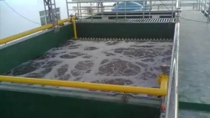
waste water treatment
2. Sources of Waste Water in PCB Manufacturing
2.1 Etching Processes
- The etching process generates copper-laden wastewater, which requires careful management to prevent heavy metal contamination.
2.2 Plating Operations
- Electroplating and immersion plating produce wastewater containing metals like nickel, gold, and silver, along with acids and alkalis.
2.3 Cleaning and Rinsing Stages
- Rinsing after solder mask application and cleaning residues from drilling processes contribute to the total wastewater volume.
3. Key Pollutants in PCB Waste Water
3.1 Heavy Metals
- Copper, lead, and nickel are the primary heavy metals found in PCB waste water.
3.2 Chemical Compounds
- Acids, alkalis, and organic solvents are common contaminants.
3.3 Suspended Solids
- Particulate matter from drilling and polishing can accumulate in the waste stream.
4. Waste Water Treatment Methods for PCB Manufacturing
4.1 Physical Treatment
- Filtration and Sedimentation: Removes suspended solids and particulate matter.
- Membrane Technology: Reverse osmosis and ultrafiltration separate contaminants from water.
4.2 Chemical Treatment
- pH Adjustment: Neutralizes acidic and alkaline waste streams.
- Precipitation and Coagulation: Removes heavy metals and other dissolved solids.
4.3 Biological Treatment
- Activated Sludge Process: Breaks down organic compounds.
- Biofilm Reactors: Uses microbial activity to reduce contamination.
5. Advanced Technologies in Waste Water Treatment
5.1 Electrocoagulation
- Uses electrical currents to remove heavy metals and other pollutants.
5.2 Advanced Oxidation Processes (AOPs)
- Decomposes organic pollutants through hydroxyl radicals.
5.3 Zero Liquid Discharge (ZLD) Systems
- Recycles water and extracts valuable materials from the waste stream.
6. Regulatory Compliance and Environmental Impact
6.1 Global Environmental Regulations
- Compliance with regulations like the US EPA Clean Water Act and European REACH standards.
6.2 Monitoring and Reporting
- Regular monitoring of pH, heavy metal concentrations, and total dissolved solids (TDS).
7. Economic and Sustainability Benefits of Waste Water Treatment
- Reduces water consumption and production costs.
- Prevents environmental penalties and enhances corporate social responsibility (CSR).
8. Future Trends and Innovations in PCB Waste Water Treatment
- Development of smart sensors for real-time monitoring.
- Implementation of machine learning for predictive maintenance.
9. Conclusion: Ensuring Sustainable PCB Manufacturing Through Effective Waste Water Treatment
In the ever-evolving landscape of electronics manufacturing, waste water treatment in PCB production is no longer an option but a necessity. As environmental regulations tighten and global sustainability goals become more pressing, PCB manufacturers must adopt comprehensive and innovative waste water management strategies.
Waste water treatment is no longer a regulatory obligation but a strategic priority for the PCB industry. By adopting advanced technologies like ZLD, AOPs, and AI-driven systems, manufacturers can achieve compliance, reduce costs, and contribute to a circular economy. As environmental standards tighten and consumer demand for green electronics grows, innovative waste water treatment solutions will define the industry’s sustainable future.
9.1 The Importance of Comprehensive Waste Water Management
Effective waste water treatment in PCB manufacturing is critical for several reasons:
- Environmental Protection: Prevents the contamination of natural water bodies with heavy metals, acids, and organic compounds.
- Regulatory Compliance: Adheres to international standards, such as the US Environmental Protection Agency (EPA) guidelines and the European Union’s Restriction of Hazardous Substances (RoHS) directive.
- Cost-Efficiency: Reduces the cost of raw materials and water consumption through recycling and reuse.
- Corporate Reputation: Enhances the company’s image as a responsible and eco-friendly manufacturer.
9.2 Current Challenges in Waste Water Treatment
Despite advancements in technology, the PCB industry faces several challenges in waste water management:
- Complex Waste Streams: PCB manufacturing involves multiple processes, such as etching, plating, and cleaning, which generate diverse contaminants.
- High Operational Costs: Advanced treatment methods like electrocoagulation and reverse osmosis require significant capital investment and maintenance.
- Regulatory Pressure: Adapting to changing environmental laws across different regions can be challenging for global manufacturers.
9.3 Solutions and Innovations for Sustainable Treatment
9.3.1 Advanced Filtration Technologies
- Membrane Bioreactors (MBRs): Combines biological treatment with membrane filtration for high-efficiency removal of organic and inorganic pollutants.
- Nanofiltration and Reverse Osmosis: Removes heavy metals and dissolved solids with high precision.
9.3.2 Chemical and Electrochemical Methods
- Electrocoagulation: Uses electrical currents to neutralize heavy metals and other toxic compounds.
- Advanced Oxidation Processes (AOPs): Employs hydroxyl radicals to break down persistent organic pollutants.
9.3.3 Biological and Eco-Friendly Approaches
- Activated Sludge Process: Utilizes microorganisms to degrade organic matter.
- Constructed Wetlands: Natural filtration systems that use plants and microbial activity to treat wastewater.
9.4 The Role of Industry Collaboration and Digitalization
9.4.1 Industry Partnerships
Collaborations between PCB manufacturers, waste water treatment companies, and environmental organizations can accelerate the development of sustainable solutions.
9.4.2 Smart Monitoring and Automation
- IoT-Based Sensors: Real-time monitoring of pH levels, heavy metal concentrations, and total dissolved solids (TDS).
- AI-Driven Predictive Analytics: Predicts potential system failures and optimizes treatment processes.
9.5 Economic and Environmental Impact
9.5.1 Cost Savings
- Reduces water usage by up to 80% through recycling.
- Lowers energy consumption and chemical usage with advanced technologies.
9.5.2 Environmental Benefits
- Minimizes hazardous waste disposal.
- Protects local ecosystems from contamination and heavy metal pollution.
9.6 Future Prospects and Global Trends
- Circular Economy Practices: Reusing treated water and recovering valuable metals from sludge.
- Green Chemistry Innovations: Developing eco-friendly chemicals and materials that reduce the need for heavy metal treatments.
- Global Standardization: Establishing universal guidelines for PCB waste water management to streamline compliance.
9.7 Final Thoughts
The future of waste water treatment in PCB manufacturing lies in a holistic and innovative approach. By investing in advanced technologies, embracing collaboration, and adhering to regulatory standards, the industry can achieve sustainability while maintaining production efficiency.
9.8 Integrating Waste Water Treatment into the PCB Production Workflow
To achieve sustainable and efficient waste water treatment in PCB manufacturing, it is crucial to seamlessly integrate treatment systems into the production line. This can be accomplished through:
9.8.1 Process-Specific Treatment Solutions
- Pre-Treatment Systems: Removing large particles and oil residues before chemical treatment.
- Segmented Waste Streams: Separating acid rinse water from metal plating solutions for targeted treatment.
- On-Site Recovery Systems: Installing metal recovery units for reclaiming copper and other valuable materials.
9.8.2 Real-Time Monitoring and Control
- Automated pH Balancing: Using sensors to monitor and adjust pH levels to optimize chemical reactions.
- Flow Rate Control: Regulating the flow of waste water to prevent overloading treatment systems.
- Data Analytics Platforms: Analyzing historical data to predict maintenance needs and optimize performance.
9.9 Case Studies of Successful Waste Water Management in PCB Manufacturing
9.9.1 Company A: Closed-Loop Water Recycling System
- Approach: Installed a reverse osmosis system to recycle rinse water.
- Results: Reduced water consumption by 70% and cut chemical waste disposal costs by 50%.
9.9.2 Company B: Electrocoagulation for Heavy Metal Removal
- Approach: Implemented electrocoagulation to remove copper and lead from plating waste water.
- Results: Achieved 95% heavy metal removal and met international discharge standards.
9.10 Regulatory Compliance and Certification
9.10.1 International Standards
- ISO 14001: Environmental management system certification.
- RoHS (Restriction of Hazardous Substances): Limiting the use of hazardous materials in electronics.
9.10.2 Local Regulations
- EPA Guidelines (U.S.): Governs the discharge of industrial waste water.
- REACH (European Union): Regulates chemical substances and their impact on the environment.
9.11 Economic Viability and ROI Analysis
9.11.1 Cost-Benefit Analysis
- Initial Investment: Capital expenditure on advanced treatment technologies.
- Operational Savings: Lower water consumption, reduced chemical use, and minimized regulatory fines.
- Long-Term ROI: Recovery of valuable metals and reduction in hazardous waste disposal fees.
9.11.2 Government Incentives and Subsidies
- Tax credits for adopting eco-friendly technologies.
- Grants for research and development in sustainable waste water treatment.
9.12 Training and Workforce Development
9.12.1 Employee Training Programs
- Educating staff on waste water treatment protocols.
- Hands-on workshops on operating advanced treatment equipment.
9.12.2 Collaboration with Environmental Experts
- Partnering with environmental engineers and consultants.
- Regular audits and assessments to ensure compliance.
9.13 Continuous Improvement and Future Roadmap
9.13.1 Innovation in Treatment Technologies
- Development of bio-based filtration systems.
- Integration of nanotechnology for selective heavy metal removal.
9.13.2 Global Collaboration for Sustainability
- Sharing best practices and technologies across the PCB manufacturing industry.
- Establishing international forums for waste water management innovation.
9.14 Conclusion: A Sustainable Path Forward
The implementation of advanced waste water treatment solutions in PCB manufacturing is not only an environmental responsibility but also a strategic advantage. By integrating cutting-edge technologies, complying with international standards, and fostering collaboration within the industry, manufacturers can achieve long-term sustainability while reducing costs and enhancing efficiency.

- long board pcb
- Flexible PCBs
- Special PCB
- Express Printed Circuit Board
- Pcb Prototype
- LED PCB
- PCB
- Printed Circuit Board
- Pcb meaning
- Pcb manufacturer
- Rigid pcb board
- Rigid Flex PCB
 Quote
Quote
 E-mail