1. Introduction to Testing Automation in PCB Manufacturing
In the rapidly evolving world of electronics manufacturing, the Printed Circuit Board (PCB) lies at the core of virtually every electronic product. From wearable health devices and smartphones to satellites and industrial control systems, the integrity and functionality of PCBs determine the overall reliability and performance of the final product. With increasing complexity in PCB architecture—such as multilayer boards, high-density interconnects (HDIs), embedded components, and rigid-flex constructions—the margin for error has shrunk dramatically. This shift has brought unprecedented emphasis on testing automation, a transformative force in ensuring PCB quality, reliability, and cost-efficiency.
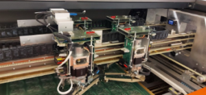
testing automation
The Complexity Challenge and the Shift from Manual Testing
As electronic devices become more compact yet more powerful, PCBs are required to host more circuitry within a smaller footprint. The intricate layouts and micro-vias that enable these designs also increase the probability of manufacturing defects, such as open circuits, short circuits, soldering errors, or misplaced components. Historically, many testing procedures were conducted manually or semi-manually, relying heavily on skilled operators using multimeters, oscilloscopes, and visual inspection. While effective in earlier decades, such techniques are no longer viable at the current scale and complexity. This reality has necessitated the introduction and rapid expansion of testing automation systems within the PCB manufacturing lifecycle.
From Quality Assurance to Strategic Competitiveness
Testing automation is not merely a quality assurance tool—it is a strategic differentiator. Modern electronics manufacturers operate in environments that demand extremely fast turnaround times, cost containment, zero-defect products, and high traceability. In such a scenario, automating test processes enables organizations to scale production while maintaining quality standards that are difficult to achieve manually. Moreover, automated systems can perform in-depth diagnostics and comprehensive testing routines faster, more accurately, and consistently than human inspectors. This shift from reactive to proactive quality assurance is a defining trait of world-class PCB manufacturers.
Beyond Speed: The Role of Precision and Repeatability
One of the cornerstones of testing automation is repeatability—the ability to perform the same test under the same conditions over time and across production batches. Manual testing inherently includes the variability of human perception and dexterity. Even a trained operator may overlook microscopic defects or produce inconsistent results depending on fatigue or environmental conditions. In contrast, automated systems leverage high-precision robotics, high-resolution imaging, and real-time feedback systems to ensure each test is executed with uniform accuracy. This precision leads to higher yield rates and significantly reduces the risk of faulty boards reaching the end customer.
Integration with Smart Manufacturing and Industry 4.0
Testing automation is also an essential building block in the journey toward Industry 4.0 and smart manufacturing. When integrated with other smart systems—such as Computer-Aided Manufacturing (CAM), Enterprise Resource Planning (ERP), and Manufacturing Execution Systems (MES)—testing automation enables a real-time, data-driven production environment. Systems can detect failures, adjust manufacturing parameters on the fly, and even predict defects using machine learning. This fusion of automation and intelligence creates closed-loop manufacturing systems that enhance productivity, optimize resource utilization, and enable near-zero defect output.
The Spectrum of Testing Automation in PCB Manufacturing
The scope of testing automation spans across several distinct methodologies, each tailored to specific defect types and stages in the PCB lifecycle:
-
Automated Optical Inspection (AOI): Uses high-resolution cameras and pattern recognition algorithms to detect visual defects like missing components, misalignments, or soldering issues.
-
In-Circuit Testing (ICT): Electrically tests individual components and circuits for performance metrics like resistance, capacitance, and functionality.
-
Flying Probe Testing: A flexible approach for low-volume and prototype testing where physical probes verify electrical continuity and performance.
-
Functional Testing (FCT): Verifies whether the assembled PCB operates correctly under expected real-world conditions.
-
Boundary Scan and JTAG Testing: Used for high-density ICs and systems where physical probe access is limited.
-
X-Ray and 3D Imaging Tests: For inspecting solder joints hidden beneath components like BGAs (Ball Grid Arrays).
Each of these testing methods can be automated to varying degrees, and most PCB manufacturers deploy a combination of them based on board complexity, production volume, and customer requirements.
Economic and Operational Implications
The upfront cost of deploying testing automation systems is often substantial. However, when evaluated over the long term, the return on investment (ROI) is significant. Benefits include reduced labor costs, faster throughput, lower defect rates, and fewer product recalls or field failures. Moreover, automated testing systems offer granular traceability and data logging—features that are invaluable for regulatory compliance, root-cause analysis, and continuous improvement programs.
Driving Forces Behind the Adoption of Testing Automation
Several macro and micro-level factors are accelerating the global adoption of testing automation in PCB production:
-
Miniaturization of Devices: Necessitates more precise and efficient testing mechanisms.
-
Increasing Product Complexity: Demands more sophisticated defect detection and diagnostics.
-
Customer Expectations: OEMs and end-users demand zero-defect delivery.
-
Regulatory Requirements: Need for traceability, documentation, and conformance to standards like IPC, ISO, and UL.
-
Supply Chain Pressures: Shorter lead times and just-in-time production models require rapid and accurate testing.
-
Sustainability Goals: Automation reduces waste, energy use, and rework, aligning with green manufacturing practices.
Cultural Shift and Workforce Transformation
Implementing testing automation also involves a cultural and workforce transformation. Traditional test engineers and quality inspectors must adapt to working alongside intelligent machines and data-centric systems. This evolution brings new career opportunities in areas such as robotics maintenance, system integration, data analytics, and software development. Training and upskilling become critical enablers of a successful automation strategy.
The Role of AI and Machine Learning in Testing Automation
The integration of artificial intelligence (AI) and machine learning (ML) into testing automation processes is transforming how PCB quality control is conducted. These technologies are especially powerful in recognizing patterns, detecting anomalies, and making predictive decisions based on vast datasets that traditional methods might overlook. In PCB testing automation, AI algorithms can be trained using historical defect data, enabling them to identify irregularities on new PCBs in real-time.
Machine learning models improve continuously as they are exposed to more testing scenarios, enhancing their accuracy and speed. For instance, an AI-driven inspection system can detect solder joint inconsistencies, missing components, or micro-cracks that human operators might miss. Over time, this not only improves the quality and reliability of PCBs but also significantly reduces inspection time and labor costs.
AI can also be used to manage testing workflows. By analyzing production trends and test outcomes, smart systems can adjust testing parameters dynamically, prioritize high-risk areas for inspection, and provide feedback for upstream manufacturing adjustments. This creates a feedback loop that contributes to process optimization across the entire PCB production line.
Cloud-Based Platforms and Remote Testing Automation in PCB Manufacturing
With increasing demands for remote operations and data accessibility, cloud-based platforms are becoming a key component of modern testing automation. Cloud integration allows for centralized control of testing procedures, data collection, and analytics. Test results from different production sites can be stored in a unified database, accessible to engineers, quality assurance teams, and stakeholders worldwide.
Remote testing automation enables test engineers to manage test systems and analyze results from virtually anywhere. This is particularly beneficial for multinational corporations or companies with distributed manufacturing facilities. Engineers can remotely calibrate testing equipment, initiate diagnostics, and assess performance metrics through secure cloud portals.
Furthermore, cloud platforms support integration with other enterprise systems like ERP (Enterprise Resource Planning) and MES (Manufacturing Execution Systems). This facilitates real-time decision-making, production planning, and traceability — all of which are crucial in today’s fast-paced and quality-focused manufacturing environments.
Human Factors and Skillsets in Testing Automation for PCBs
Despite the high level of automation, human expertise remains essential in developing, maintaining, and improving testing automation frameworks. Engineers must design and validate testing algorithms, interpret ambiguous results, and make decisions in non-standard situations. This shift changes the role of human workers from manual testers to automation specialists, requiring a new set of skills in software development, data analytics, and system integration.
Training becomes a critical component in the successful implementation of testing automation. Staff must understand not only how to operate automated equipment but also how to interpret data, adjust parameters, and troubleshoot issues that may arise. Investing in workforce development ensures that automation tools are used to their fullest potential and that the system remains flexible and adaptable.
Moreover, collaboration between hardware engineers, software developers, and quality assurance teams is more important than ever. A multidisciplinary approach is required to ensure that testing strategies align with product design requirements, production capabilities, and business objectives.
Conclusion: The Future and Impact of Testing Automation in PCB Manufacturing
As the demand for complex, miniaturized, and high-performance electronics continues to rise across global industries—from aerospace and automotive to medical devices and consumer gadgets—the role of testing automation in PCB manufacturing is becoming more crucial than ever. While this article has explored the tools, processes, challenges, and methodologies surrounding automated PCB testing, it’s equally important to reflect on the broader impact this technological evolution is having on quality, cost-efficiency, and industry standards.
Transformational Impact on Production Quality and Reliability
One of the most profound contributions of testing automation is the dramatic improvement in product quality and reliability. Automated systems can conduct rigorous tests with far greater consistency than manual operators, identifying even the most subtle anomalies across thousands of units per day. In industries where a single PCB failure could lead to mission-critical system breakdowns, such as in avionics or implantable medical electronics, this capability cannot be overstated.
Moreover, as the number of components per board increases and board layouts grow in complexity, human testing becomes increasingly inadequate. Automated systems are uniquely capable of handling high-density interconnects, microvias, and multilayer stack-ups without compromising inspection depth. This leads to higher confidence in the final product and reduced field returns, warranty claims, and brand damage.
Enhanced Manufacturing Throughput and Operational Efficiency
Another key advantage of automated testing lies in its ability to drastically increase throughput. With parallel testing channels, automated fixture-based platforms, and intelligent software integration, manufacturers can test thousands of boards in the time it would take a human operator to test just a few dozen. This scalability is especially critical for meeting tight lead times in mass production scenarios.
Moreover, testing automation allows for real-time data capture and analysis. Manufacturers can use these insights to adjust upstream processes proactively, eliminating defects before they propagate further down the line. This closed-loop feedback mechanism helps reduce rework and scrap, while supporting lean manufacturing initiatives and reducing the environmental footprint.
Cost Optimization and Long-Term Return on Investment
Although the initial setup of a testing automation infrastructure involves capital investment in machinery, software, and operator training, the long-term financial benefits are significant. By eliminating manual labor costs, reducing test cycle time, and minimizing scrap and rework, automation drives down the cost-per-unit over time. Additionally, the improved yield and reduction in RMA (Return Merchandise Authorization) claims can have a tangible effect on profitability.
For small and medium-sized enterprises, modular and scalable testing platforms now offer an accessible pathway to automation without requiring massive upfront capital. Cloud-connected solutions and AI-powered optimization algorithms are also making it possible to derive insights without needing large in-house engineering teams.
Technology Integration and the Rise of Smart Manufacturing
The role of testing automation extends beyond individual machines and into the broader digital transformation of the PCB manufacturing ecosystem. Modern automated test systems are being seamlessly integrated into MES (Manufacturing Execution Systems), ERP (Enterprise Resource Planning) software, and factory-level IoT networks. This integration is a foundational component of smart manufacturing and Industry 4.0 strategies.
For example, a failing test result on a specific board trace can trigger immediate alerts, isolate the defective lot, and even adjust upstream processes such as solder paste deposition or pick-and-place programming. The interconnectivity between machines and processes promotes a predictive maintenance model, minimizes production downtime, and supports agile manufacturing capabilities.
Human Factors: Shifting Roles in a Digitally Driven Environment
While automation reduces the need for manual testing, it doesn’t eliminate the need for human expertise. Instead, it shifts the focus from repetitive tasks to more analytical, supervisory, and strategic roles. Technicians and engineers are now required to interpret diagnostic data, fine-tune algorithms, design test strategies, and maintain complex equipment.
The new skill sets required include software integration, data analytics, machine learning, and test engineering. Upskilling the workforce is thus an essential companion to automation. PCB manufacturers must invest not only in technology but also in training and retaining qualified personnel who can operate, troubleshoot, and improve automated systems.
Challenges and Risk Management in Testing Automation
Despite its many advantages, testing automation is not without its challenges. One key issue is the risk of “false negatives” or “false positives” resulting from improperly calibrated systems or overly rigid test thresholds. If not managed properly, these can lead to unnecessary board rejection or the passing of defective units.
Moreover, the dependency on high-tech equipment introduces vulnerability to system failures or cyber threats. Manufacturers must establish robust quality assurance protocols, equipment maintenance schedules, and cybersecurity safeguards to ensure uninterrupted and safe operations.
Additionally, test coverage remains a critical concern. While automation improves efficiency, it must not compromise the depth and breadth of testing. Striking the right balance between test time, coverage, and cost remains one of the most complex aspects of automated test engineering.
Outlook: Future Trends in Testing Automation
Looking ahead, the trajectory of testing automation in PCB manufacturing is aligned with several exciting technological developments:
-
AI and Machine Learning Integration: Smart test algorithms will be able to adapt in real-time, reducing test times while increasing defect detection accuracy.
-
Digital Twin Technology: Simulated test environments will allow virtual validation of PCB designs before physical production begins.
-
Robotic Test Execution: Highly dexterous robots with integrated sensors will perform multi-angle, multi-point tests without human intervention.
-
Cloud-Based Test Data Repositories: Cross-facility data collection and comparison will enable predictive analytics, benchmarking, and global quality management.
These advances will redefine what’s possible in terms of speed, scalability, customization, and intelligence in PCB manufacturing and testing.
Conclusion: Strategic Imperative for the Electronics Industry
In conclusion, testing automation in PCB manufacturing is not just a technological upgrade—it’s a strategic imperative. In a global market where speed, quality, and innovation determine competitiveness, automation ensures that PCB manufacturers can meet modern expectations without compromise. From quality assurance to cost control, from workforce development to digital transformation, testing automation is a linchpin of the future-ready electronics supply chain.
As testing tools continue to evolve—becoming faster, smarter, and more interconnected—their value will extend far beyond defect detection. They will become central to decision-making, customer satisfaction, and continuous improvement. The journey toward fully automated, intelligent testing is well underway, and the manufacturers that embrace it will shape the future of electronics.

- long board pcb
- Flexible PCBs
- Special PCB
- Express Printed Circuit Board
- Pcb Prototype
- LED PCB
- PCB
- Printed Circuit Board
- Pcb meaning
- Pcb manufacturer
- Rigid pcb board
- Rigid Flex PCB
 Quote
Quote
 E-mail