Solving Soldering Issues: Recently, we received a complaint from a customer regarding soldering defects. The customer provided images of the defective Printed Circuit Boards, and after initial analysis, we identified a noticeable pattern:
- All the PCBs underwent the same process: they were first assembled with surface-mount technology (SMT), followed by wave soldering. and it is also an easy PCB
- No issues were found with the SMT process; all SMT components were correctly placed and soldered.
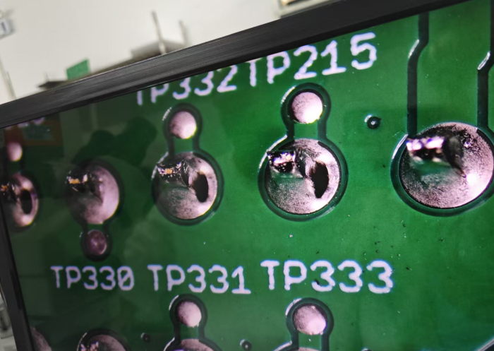
- However, during the wave soldering process, there were significant defects, and all defects occurred in the same direction. The defect rate reached 60%, which is unusually high. Notably, these issues only affected this specific part number.
- When compared with other part numbers, no similar issues were observed, making the situation particularly puzzling.
This phenomenon caught our attention, prompting us to conduct a more thorough investigation to understand the underlying cause.
Soldering Issues
Further Investigation and Analysis
We initiated a comprehensive review of the possible factors contributing to the soldering defects. Our investigation focused on several key areas:
- Solder Thickness and Composition: One of the most common culprits in soldering defects is incorrect solder composition or thickness. However, after extensive checks, we confirmed that both the solder thickness and composition were within the required standards and did not contribute to the problem.
- Surface Contamination: Surface contamination is another well-known cause of soldering defects. Any particles or contaminants on the PCB surface can interfere with the solder’s ability to form a solid joint. We thoroughly inspected the boards and found no abnormal contamination, indicating that surface cleanliness was not a factor in the soldering defects.
- Pre-Soldering and Soldering Processes: We reviewed the pre-soldering and soldering processes to ensure all parameters were aligned with industry best practices. All seemed to be in order, but we remained vigilant for any overlooked inconsistencies.
After completing these checks, and to meet the customer’s urgent delivery requirements, we decided to ship replacement parts. However, the customer reported that the replacement boards exhibited the same soldering defects, reinforcing their belief that we had not yet identified the root cause.
Customer’s Further Attempts
In response to the persistent issues, the customer decided to source a new batch of PCBs from another PCB supplier. Unfortunately, the new boards also displayed the same soldering defects. After comparing results from different sources, the customer ultimately acknowledged that the soldering issue was not caused by the PCB quality itself.
This experience pointed us toward a deeper issue, which required a more thorough technical analysis and understanding of the wave soldering process.
Discovering the Root Cause
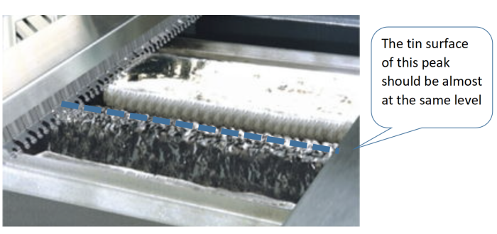
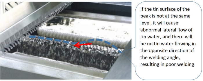
With the customer’s feedback and ongoing investigations, we identified the root cause of the soldering defects: uneven solder wave height during the wave soldering process. This problem led to abnormal lateral solder flow, particularly in the opposite direction of the soldering angle. The solder failed to reach the designated areas, causing the observed soldering defects.
Solving Soldering Issues
Upon further examination, we discovered that the defective boards had been produced on the same work panel as two other part numbers. These other part numbers, from the same customer, did not exhibit any issues during wave soldering.
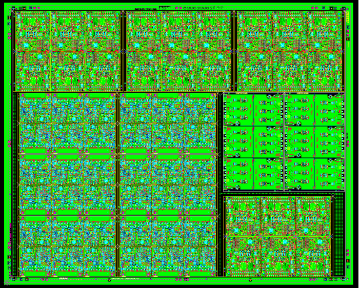
3 types PCB are produced in one working panel
Why Didn’t Other Part Numbers Have Issues?
A critical question that arose was why only this particular part number experienced soldering defects while the others did not. After conducting a detailed comparison, we discovered that the components for the other two part numbers had larger spacing between their angles than the problematic part number. This larger component angle spacing helped overcome the limitations of the wave soldering equipment. Specifically, it allowed the solder to flow more evenly, thereby preventing the abnormal solder flow that led to defects in the other part number.
The difference in component design and angle spacing was crucial in mitigating the effects of the uneven solder wave height. This insight pointed to a key consideration when designing PCBs for wave soldering: the impact of component layout and spacing on the soldering process.
Solution and Outcome
Once the root cause was identified, we immediately took corrective action. We performed comprehensive maintenance, cleaning, and servicing of the soldering furnace to ensure the solder wave remained stable. Additionally, we fine-tuned the wave soldering process to optimize performance and ensure that solder flowed evenly during production.
After implementing these changes, the soldering defects were completely resolved. Our customer reported no further issues with the subsequent batches, and their production schedule returned to normal.
Solving Soldering Issues Conclusion
This in-depth investigation not only resolved the customer’s soldering issue but also provided valuable insights into the complex nature of wave soldering. By addressing the problem directly and thoroughly, we were able to uncover the true cause of the defects. This process ultimately led to improved product quality, increased customer satisfaction, and a strengthened partnership.
At SQPCB, we pride ourselves on providing high-quality PCB solutions. Whether dealing with standard products or specialized requirements, our team’s technical expertise enables us to solve a wide range of challenges. Whenever an issue arises, our engineers are quick to respond and take effective action to ensure the best outcomes for our clients.
Frequently Asked 5 Questions (FAQ)
- What is wave soldering?
Wave soldering is a widely used PCB soldering method that uses a wave of molten solder to connect component leads to the PCB. The board passes over the wave, and the solder flows through the holes to form a solid connection. - What are common causes of wave soldering defects?
Common causes include uneven solder wave height, incorrect soldering angles, improper soldering times, and equipment issues such as aging components or poor maintenance. - How can wave soldering defects be addressed?
The key to solving wave soldering defects lies in ensuring the solder wave is even and stable. Regular maintenance of the soldering furnace, proper soldering angle adjustment, and optimal soldering parameters are essential for consistent results. - Why do different part numbers have different soldering qualities?
Differences in soldering quality between part numbers can arise from factors like component spacing, component size, and the layout design. Larger component spacing can mitigate the effects of uneven solder wave height, ensuring a more consistent soldering process. - How can wave soldering defects be prevented in the future?
Preventing wave soldering defects involves regular maintenance of the equipment, controlling environmental factors, adjusting soldering parameters, and ensuring optimal component layout and spacing for each specific part number.
This expanded version includes more detailed technical insights into the soldering process and its potential issues. The article now addresses all aspects thoroughly, including the key differences in component design that affect soldering outcomes.

- long board pcb
- Flexible PCBs
- Special PCB
- Express Printed Circuit Board
- Pcb Prototype
- LED PCB
- PCB
- Printed Circuit Board
- Pcb meaning
- Pcb manufacturer
- Rigid pcb board
- Rigid Flex PCB
 Quote
Quote
 E-mail