Introduction to Solder Pad in PCB Manufacturing
In the complex process of PCB manufacturing, the solder-pad serves as one of the most critical components. Although it seems like a small and simple feature, the solder-pad plays a pivotal role in determining the electrical connectivity, mechanical stability, and overall reliability of a printed circuit board. A solder-pad is essentially a conductive area, usually made of copper, designed to provide a point of electrical connection for component leads, pins, or terminals during the soldering process.
Understanding the Functionality of Solder-Pad
The solder-pad functions as the physical anchor that ensures electronic components are securely mounted on the PCB. Without a properly designed and manufactured solder pad, the solder joints would be prone to failure, leading to intermittent connections or total circuit failure. This small feature must withstand various mechanical, chemical, and thermal stresses throughout the product’s lifecycle.
In modern PCB manufacturing, solder-pad quality has become even more critical due to the miniaturization of components, the adoption of fine-pitch designs, and the increasing demands for high-density interconnect (HDI) structures. A failure in the solder-pad can render the entire assembly non-functional, which is particularly unacceptable in industries such as aerospace, automotive, and medical devices, where reliability is paramount.
The Complexity of Solder-Pad Problems
Despite technological advances, solder-pad issues remain common in PCB production. Problems may arise from poor design, improper material selection, suboptimal manufacturing processes, or even environmental factors such as humidity and temperature variations during storage and assembly. Typical issues include solder-pad peeling, misalignment, oxidation, cracking, and contamination, each capable of significantly compromising product quality.
In high-reliability applications, even minor defects in the solder-pad can escalate into major failures over time. For this reason, manufacturers must pay close attention to each stage of the solder pad lifecycle, from design and material selection to processing, assembly, and final testing.
Importance of Proactive Solutions
Addressing solder pad problems requires a proactive approach that integrates design for manufacturability (DFM), robust process control, and stringent quality assurance practices. With proper techniques and attention to detail, many of the common solder-pad problems can be mitigated or entirely prevented. Solutions such as improving surface finishes, optimizing pad geometries, and applying advanced cleaning processes have proven effective in enhancing solder-pad reliability.
From my perspective, engineers and PCB designers should develop a holistic understanding of the causes and solutions associated with solder-pad issues. This will not only improve the success rate of first-pass manufacturing but will also contribute to long-term product reliability and customer satisfaction.
A Roadmap for Problem-Solving
In the following sections of this article, I will provide an in-depth analysis of various solder-pad problems encountered in PCB manufacturing, along with practical solutions and my own reflections based on industry practices. By exploring the intricate relationship between design, material science, and manufacturing processes, we can develop comprehensive strategies to overcome these challenges.
The ultimate goal is to empower PCB professionals with knowledge that can reduce failure rates, enhance product quality, and ensure that solder-pad performance aligns with the high expectations of today’s advanced electronics.
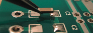
solder Pad
Common Design Problems of Solder Pad in PCB Manufacturing
Introduction to Design Challenges of Solder-Pad in PCB Manufacturing
One of the most frequent sources of solder-pad problems in PCB manufacturing stems from the design stage. Even when materials and processing are optimized, a poorly designed solder-pad can compromise the entire assembly. Design engineers must carefully balance component specifications, manufacturing capabilities, and reliability requirements to ensure that the solder-pad performs as intended.
In this section, we will explore the most common design issues associated with the solder-pad in PCB manufacturing, as well as discuss effective strategies to address these challenges.
Inadequate Solder-Pad Size in PCB Manufacturing
One of the most overlooked design issues is the improper sizing of the solder-pad. When a solder-pad is too small, it may not provide enough area for proper solder wetting, leading to weak joints that can crack under mechanical stress or thermal cycling. Conversely, a solder-pad that is too large can cause excessive solder accumulation, creating the risk of solder bridging and short circuits.
Solutions:
-
Use IPC standards as a reference for recommended solder-pad dimensions.
-
Validate the solder-pad size through thermal simulations to ensure proper heat dissipation and solder flow.
-
Perform design rule checks (DRC) to identify potential size violations before moving to fabrication.
Incorrect Solder-Pad Spacing in PCB Manufacturing
Insufficient spacing between adjacent solder-pads can increase the risk of solder bridging, especially in fine-pitch components. This is particularly problematic when automated solder paste printing and reflow processes are used.
Solutions:
-
Maintain minimum clearance requirements as per IPC standards for the specific component package.
-
For fine-pitch designs, consider using solder mask defined (SMD) solder-pads to better control solder flow and prevent bridging.
-
Simulate the solder paste printing process to assess the potential for solder overflow.
Improper Solder Pad Geometry in PCB Manufacturing
The geometry of the solder-pad affects not only solderability but also mechanical stability. Sharp corners in solder-pad design can become stress concentration points, leading to pad lifting or cracking over time.
Solutions:
-
Use rounded corners instead of sharp ones to distribute mechanical stress evenly.
-
Ensure that the solder-pad geometry matches the thermal and mechanical behavior of the intended component.
-
Adopt teardrop-shaped solder-pads in high-density designs to reinforce connections at trace-to-pad junctions.
Misaligned Solder-Pad Layout in PCB Manufacturing
Improper alignment between the solder-pad and the corresponding component leads can result in defective solder joints, cold soldering, or open circuits. This misalignment may originate from component footprint errors or design database inconsistencies.
Solutions:
-
Verify all component footprints in the PCB library against manufacturer datasheets.
-
Conduct optical alignment checks in the assembly process to detect and correct placement errors.
-
Implement design-for-assembly (DFA) principles to account for manufacturing tolerances and alignment variability.
Lack of Thermal Relief in Solder-Pad Design in PCB Manufacturing
A solder-pad that connects directly to large copper planes without thermal relief may not reach proper soldering temperatures during reflow. This issue can cause incomplete soldering or weak joints.
Solutions:
-
Add thermal relief patterns to the solder-pad connections to regulate heat flow during soldering.
-
Balance the thermal mass across the board to prevent uneven heating.
-
Simulate reflow profiles to ensure adequate temperature distribution on all solder-pads.
Inadequate Via Placement near Solder Pad in PCB Manufacturing
Placing vias too close to or within the solder-pad area can cause solder wicking into the via, resulting in insufficient solder on the solder-pad itself. This is especially problematic for via-in-pad designs when not properly managed.
Solutions:
-
Avoid via-in-pad configurations unless specifically required by design constraints.
-
Use via tenting or via plugging techniques to prevent solder from draining into the vias.
-
If via-in-pad is necessary, ensure proper filling and planarization to support reliable soldering.
Lack of Solder Mask Clearance in Solder Pad Design in PCB Manufacturing
When the solder-pad is not properly defined in relation to the solder mask, it can lead to unintended solder mask covering the pad, which will inhibit proper solder adhesion.
Solutions:
-
Ensure adequate solder mask clearance based on component size and placement precision.
-
Use solder mask defined (SMD) or non-solder mask defined (NSMD) strategies based on the specific application and reliability needs.
-
Perform design checks using automated design software to validate solder mask openings.
My Reflections on Solder Pad Design in PCB Manufacturing
Through years of exposure to PCB design and production, I’ve realized that solder-pad issues often originate from decisions made during the initial design phase. Some designers tend to focus solely on fitting the electrical components without fully considering manufacturing constraints and assembly tolerances. This lack of alignment between design and production teams frequently results in solder-pad problems that could have been avoided with better cross-functional collaboration.
In my view, a highly effective strategy is to involve process engineers early in the design cycle, allowing them to provide valuable input on solder-pad geometry, spacing, and thermal management. Furthermore, modern PCB design software offers simulation tools that can predict solder paste behavior and reflow profiles. Utilizing these tools early can significantly reduce the risk of solder-pad failures later in the manufacturing process.
Material-Related Problems of Solder Pad in PCB Manufacturing
Introduction to Material Selection for Solder Pad in PCB Manufacturing
Material selection is a foundational element that directly influences the performance and reliability of the solder pad in PCB manufacturing. Even with perfect design and process control, if the materials used for the solder-pad are substandard or incompatible with the overall assembly, failure is almost inevitable.
This section focuses on common material-related challenges that affect the solder pad in PCB manufacturing and practical solutions to address them effectively.
Poor Copper Foil Quality Affecting Solder Pad in PCB Manufacturing
The solder pad is typically formed from copper foil laminated onto the PCB substrate. If the copper foil is of poor quality—such as having uneven thickness, low peel strength, or high impurity content—the solder pad becomes vulnerable to adhesion failure, peeling, and cracking.
Solutions:
-
Source high-quality copper foil that meets IPC-4562 standards for base materials.
-
Ensure the copper foil has consistent thickness and high purity to support good solderability and mechanical stability.
-
Establish stringent supplier qualification processes to guarantee material reliability.
Substrate Incompatibility Impacting Solder Pad in PCB Manufacturing
The interaction between the PCB substrate and the solder-pad is critical. For example, certain high-temperature substrates may expand at a rate different from the copper, causing mechanical stress that can lead to solder-pad detachment.
Solutions:
-
Match the coefficient of thermal expansion (CTE) of the copper foil and the substrate to minimize thermal stress.
-
Choose substrate materials like high-Tg FR4 or polyimide for high-temperature applications.
-
Conduct thermal shock testing to validate substrate and solder-pad compatibility.
Low-Quality Surface Finishes on Solder Pad in PCB Manufacturing
Surface finishes such as HASL (Hot Air Solder Leveling), ENIG (Electroless Nickel Immersion Gold), or OSP (Organic Solderability Preservative) play a crucial role in protecting the solder-pad from oxidation and ensuring good solderability. Poor surface finish quality can lead to soldering defects and reliability issues.
Solutions:
-
Select surface finishes appropriate to the end-use environment and component type.
-
For fine-pitch applications, prefer ENIG or OSP over HASL to achieve flatter solder-pads.
-
Ensure tight control over the surface finish process to avoid uneven plating, poor adhesion, or surface contamination.
Contaminated Base Material Causing Solder Pad Issues in PCB Manufacturing
If the PCB base material or copper foil is contaminated with oils, debris, or chemical residues during manufacturing, the solder-pad may suffer from poor solder adhesion or complete soldering failure.
Solutions:
-
Implement strict cleanliness protocols in material handling and storage areas.
-
Use chemical cleaning and plasma treatment to remove contaminants from the solder-pad surface prior to solder mask application.
-
Verify cleanliness using surface insulation resistance (SIR) and ionic contamination testing.
Inappropriate Copper Thickness in Solder Pad in PCB Manufacturing
Using copper that is too thin may result in a solder-pad that lacks mechanical strength, while overly thick copper can cause excessive heat absorption and uneven solder flow.
Solutions:
-
Use standard copper thickness (e.g., 1 oz or 35 μm) for most applications unless otherwise required.
-
For high-current or high-power circuits, select appropriate copper weights (e.g., 2 oz or 70 μm) but ensure thermal profiles are adjusted accordingly.
-
Validate copper thickness using cross-sectional analysis during incoming quality control.
Inconsistent Laminate Resin Distribution Affecting Solder Pad in PCB Manufacturing
Uneven resin distribution in the PCB laminate can result in voids or resin starvation under the solder-pad, which weakens adhesion and increases the likelihood of pad lifting.
Solutions:
-
Work with laminate suppliers to ensure resin flow consistency.
-
Inspect multilayer lamination parameters to control pressure, heat, and resin flow uniformly across the board.
-
Utilize X-ray inspection to detect voids or resin deficiency beneath the solder-pad areas.
My Reflections on Solder Pad Material Selection in PCB Manufacturing
In my experience, material selection for solder-pads is often underestimated in PCB projects where cost pressures dominate decision-making. Manufacturers sometimes opt for lower-cost copper foils or surface finishes to meet price targets, without fully considering the long-term reliability trade-offs. This short-sighted approach can lead to costly field failures, product recalls, and damaged customer relationships.
I believe that investing in higher-grade materials for the solder-pad, especially for mission-critical applications, yields much better lifecycle performance and customer satisfaction. Cost reduction strategies should focus more on process efficiency rather than compromising on core material quality.
Close collaboration between designers, material engineers, and suppliers is essential to optimize solder-pad material choices that balance cost, performance, and reliability.
Solder Pad Adhesion Issues in PCB Manufacturing
Introduction to Solder Pad Adhesion Issues in PCB Manufacturing
Among the many challenges in PCB manufacturing, solder-pad adhesion issues are some of the most common and concerning. When a solder-pad fails to adhere properly to the PCB substrate, it can cause significant defects such as pad lifting, intermittent connections, and total circuit failure, especially after soldering, thermal cycling, or mechanical stress.
This section provides an in-depth exploration of solder-pad adhesion problems in PCB manufacturing, their root causes, practical solutions, and personal insights based on real-world manufacturing practices.
Inadequate Lamination Process Affecting Solder Pad Adhesion in PCB Manufacturing
The lamination process directly impacts the bonding between the copper foil and the PCB substrate. If the lamination temperature, pressure, or time is not well controlled, it can cause poor adhesion between the solder-pad and the substrate, which may result in pad lifting during subsequent soldering or rework processes.
Solutions:
-
Carefully monitor and control lamination process parameters such as temperature ramp rate, lamination pressure, and cooling rate.
-
Use reliable lamination presses with uniform pressure distribution to ensure consistent bonding across the PCB.
-
Perform peel strength testing to validate copper adhesion on sample panels.
Contaminants on Copper Surface Reducing Solder Pad Adhesion in PCB Manufacturing
Surface contaminants such as oxidation, oils, or particulate debris present on the copper foil before lamination can severely weaken solder-pad adhesion.
Solutions:
-
Implement thorough pre-cleaning processes including micro-etching and deoxidization to prepare the copper surface.
-
Ensure a cleanroom environment or controlled areas during critical lamination steps.
-
Verify cleanliness through ionic contamination testing and surface energy measurements.
Inadequate Surface Roughness of Copper Affecting Solder Pad Adhesion in PCB Manufacturing
Copper surfaces with insufficient roughness can result in weak mechanical interlocking between the copper and resin, which reduces solder-pad adhesion strength.
Solutions:
-
Apply controlled micro-etching or black oxide treatments to achieve optimal surface roughness.
-
Validate surface topography using profilometry to ensure the copper roughness falls within required specifications.
-
Use advanced adhesion promoters compatible with the specific PCB resin system.
Delamination Due to Thermal Stress on Solder Pad in PCB Manufacturing
Rapid temperature changes during reflow soldering or thermal shock can induce expansion mismatch between copper and the substrate, causing solder-pad delamination.
Solutions:
-
Select substrates with low CTE (coefficient of thermal expansion) to minimize stress on the solder-pad.
-
Design thermal profiles carefully to avoid excessive heating rates and uneven cooling.
-
Apply thermal relief patterns in the design to buffer heat flow and reduce mechanical stress concentrations.
Excessive Mechanical Force During Assembly Impacting Solder Pad Adhesion in PCB Manufacturing
During component placement or manual handling, excessive force can mechanically damage the solder-pad and weaken its adhesion to the PCB substrate.
Solutions:
-
Set appropriate force limits on pick-and-place machines to prevent over-compression on sensitive solder-pads.
-
Implement operator training programs to reduce the risk of manual handling damage.
-
Use tooling and fixturing that supports the PCB properly during assembly and soldering processes.
Moisture Absorption Leading to Solder-Pad Adhesion Failure in PCB Manufacturing
If the PCB absorbs moisture prior to soldering, rapid vaporization during reflow can cause internal delamination or pad lifting.
Solutions:
-
Implement strict moisture sensitivity level (MSL) controls and follow pre-baking protocols for moisture removal.
-
Store PCBs in vacuum-sealed or dry cabinets to prevent moisture ingress.
-
Conduct cross-sectional inspections after soldering to check for delamination signs.
Inadequate Resin Flow Beneath Solder Pad in PCB Manufacturing
If the PCB resin does not fully wet or encapsulate the copper during lamination, it can leave voids beneath the solder pad that compromise adhesion.
Solutions:
-
Optimize resin flow properties by selecting suitable prepreg materials.
-
Control lamination cycles to ensure complete resin fill, especially for multilayer boards.
-
Use X-ray or ultrasonic inspection to detect voids or incomplete resin coverage.
My Reflections on Solder-Pad Adhesion in PCB Manufacturing
Over the years, I have witnessed how minor lapses in process control can lead to significant solder-pad adhesion issues, often discovered too late during final assembly or field use. One particular challenge I’ve seen repeatedly is manufacturers underestimating the role of moisture control and proper surface preparation, which directly impacts solder-pad bonding strength.
I believe that achieving robust solder-pad adhesion requires a holistic approach: strict material inspection, optimized lamination processes, rigorous environmental control, and detailed assembly handling procedures. Additionally, preventive inspections like peel testing and cross-section analysis should be part of the standard quality control process rather than optional verification steps.
Manufacturers that consistently apply these proactive measures tend to experience far fewer solder-pad adhesion failures and generally achieve higher field reliability.
Solder Pad Peeling Problems in PCB Manufacturing
Introduction to Solder-Pad Peeling Problems in PCB Manufacturing
Solder pad peeling is one of the most critical failure modes in PCB manufacturing. When the solder-pad detaches from the PCB substrate, it often results in an open circuit, rendering the entire assembly either defective or unreliable. Peeling can occur during manufacturing, rework, or even during the product’s operational life.
In this section, we will comprehensively examine the common causes of solder-pad peeling in PCB manufacturing, explore proven solutions, and share my own reflections on how to prevent such failures.
Thermal Shock as a Cause of Solder Pad Peeling in PCB Manufacturing
One of the most frequent causes of solder-pad peeling is rapid thermal shock, especially during processes like wave soldering, reflow soldering, or thermal cycling in environmental stress testing.
Solutions:
-
Gradually ramp up and cool down temperatures in thermal profiles to reduce stress on the solder-pad.
-
Use high-Tg and low-CTE substrates to minimize the expansion mismatch between the copper and the PCB base material.
-
Conduct thermal shock resistance testing to validate the PCB’s ability to withstand rapid temperature changes.
Mechanical Stress Leading to Solder Pad Peeling in PCB Manufacturing
Mechanical forces applied during component insertion, handling, or assembly can damage the solder-pad and cause it to peel, especially if the copper adhesion to the substrate is already weak.
Solutions:
-
Employ automated assembly equipment with controlled insertion and placement force to prevent stress on solder-pads.
-
Provide proper mechanical support under the PCB during assembly to minimize flexing.
-
Train operators to handle PCBs carefully and avoid bending or applying force directly to sensitive areas.
Inadequate Copper Adhesion Causing Solder Pad Peeling in PCB Manufacturing
Poor copper adhesion is a fundamental cause of solder-pad peeling, often resulting from issues in the lamination or surface preparation stages.
Solutions:
-
Ensure copper foil surfaces are properly roughened to promote resin bonding.
-
Implement consistent lamination pressure and temperature to achieve strong copper-to-substrate adhesion.
-
Perform periodic peel strength testing to confirm adhesion meets manufacturing standards.
Excessive Rework Leading to Solder Pad Peeling in PCB Manufacturing
Repeated heating, desoldering, or component removal can degrade the solder pad’s adhesion, leading to peeling.
Solutions:
-
Minimize rework cycles and apply strict thermal management during any rework process.
-
Use appropriate rework tools that provide localized heat to avoid unnecessary thermal stress on the PCB.
-
Avoid repeated soldering on the same solder pad whenever possible.
Contaminated Surfaces Causing Solder Pad Peeling in PCB Manufacturing
Surface contamination, including oxidation, dust, or chemical residues, can interfere with copper adhesion and promote solder pad peeling during thermal or mechanical stress.
Solutions:
-
Implement thorough cleaning and surface preparation prior to lamination.
-
Use pre-lamination plasma treatment to increase surface energy and improve resin adhesion.
-
Store materials and semi-finished boards in clean, controlled environments to prevent contamination.
Moisture Entrapment Causing Solder Pad Peeling in PCB Manufacturing
When moisture is trapped within the PCB layers, rapid heating during soldering can cause vapor expansion, leading to internal delamination and solder pad peeling.
Solutions:
-
Store PCBs in dry cabinets or vacuum-sealed packaging to prevent moisture absorption.
-
Bake PCBs at recommended temperatures before assembly to remove residual moisture.
-
Monitor humidity levels in storage and assembly areas to reduce moisture risk.
Substrate Degradation Contributing to Solder Pad Peeling in PCB Manufacturing
Low-quality substrates or those exposed to excessive thermal stress can degrade over time, weakening their ability to hold the solder pad securely.
Solutions:
-
Select substrates with proven thermal and mechanical reliability.
-
Validate long-term aging and thermal cycling performance during product development.
-
Use substrates with enhanced resin systems that provide better copper adhesion.
Improper Hole Wall Quality Causing Solder Pad Peeling in PCB Manufacturing
When the drilled hole walls in plated through holes (PTH) are rough or damaged, they can introduce mechanical weaknesses that cause solder pad peeling around via areas.
Solutions:
-
Use high-precision drilling techniques with optimized parameters to minimize burrs and roughness.
-
Control desmear and hole preparation processes to ensure smooth, high-quality barrel walls.
-
Regularly inspect drilled holes for quality consistency using optical or cross-sectional analysis.
My Reflections on Solder Pad Peeling in PCB Manufacturing
From my practical experience, solder pad peeling is one of the most preventable yet frequently encountered issues in PCB manufacturing. I have seen that even well-designed PCBs can suffer from peeling when process discipline is lacking—whether it’s due to poorly controlled rework, unmonitored lamination pressure, or inadequate material storage.
In my opinion, the key to minimizing solder pad peeling is not just process control but also operator education and cross-functional collaboration. Operators must understand that PCB handling and rework techniques directly influence pad integrity. Engineers must design boards that account for realistic assembly stresses and thermal cycles.
It is also vital to foster a manufacturing culture that prioritizes prevention over correction. By using advanced inspection methods, proactive moisture management, and improved assembly guidelines, manufacturers can significantly reduce the occurrence of solder pad peeling and improve product reliability.
Solder Pad Oxidation Problems in PCB Manufacturing
Introduction to Solder Pad Oxidation Problems in PCB Manufacturing
Oxidation is a common surface defect that can severely compromise the performance and reliability of the solder pad in PCB manufacturing. When the solder pad surface becomes oxidized, it inhibits proper solder wetting, leading to cold solder joints, increased contact resistance, and in severe cases, total soldering failure. Oxidation can occur at multiple stages, including material storage, PCB fabrication, and assembly.
This section will explore the key causes, solutions, and practical considerations regarding solder pad oxidation in PCB manufacturing, alongside my own reflections from hands-on experience.
Inadequate Storage Conditions Leading to Solder Pad Oxidation in PCB Manufacturing
One of the most frequent causes of solder pad oxidation is improper storage of bare PCBs. Exposure to humidity, oxygen, and temperature fluctuations can quickly form oxide layers on the solder pad surface.
Solutions:
-
Store PCBs in vacuum-sealed, nitrogen-filled, or moisture-barrier packaging to prevent exposure to air and humidity.
-
Use desiccants and humidity indicator cards in PCB packaging to actively monitor moisture levels.
-
Maintain storage environments at controlled temperatures and low relative humidity to minimize oxidation risk.
Delays Between Surface Finishing and Assembly Increasing Solder Pad Oxidation in PCB Manufacturing
The longer the delay between PCB surface finish application and assembly, the higher the risk of solder pad oxidation, especially for surface finishes like HASL and bare copper.
Solutions:
-
Minimize the time between surface finish application and assembly processes.
-
Prefer surface finishes like ENIG, ENEPIG, or OSP that provide better oxidation resistance over extended storage periods.
-
If PCBs are stored for extended periods, perform solderability testing prior to use to verify the condition of the solder pad surface.
Use of Reactive Surface Finishes Contributing to Solder Pad Oxidation in PCB Manufacturing
Some surface finishes, such as bare copper or HASL, are more susceptible to oxidation than others. Improper handling of these finishes can accelerate oxidation and compromise solderability.
Solutions:
-
Select oxidation-resistant finishes such as ENIG or OSP for sensitive or high-reliability applications.
-
Handle PCBs with gloves or vacuum tools to prevent contamination from skin oils, which can promote oxidation.
-
Store PCBs with sensitive finishes in nitrogen cabinets to minimize oxygen exposure.
Inadequate Cleaning After Etching Causing Solder Pad Oxidation in PCB Manufacturing
Residues left on the PCB surface after chemical etching can react with environmental moisture, promoting oxidation of the solder pad.
Solutions:
-
Implement effective post-etch cleaning protocols to remove residues and reduce ionic contamination.
-
Use deionized water rinsing and drying processes to eliminate chemicals that could trigger oxidation.
-
Validate surface cleanliness through ionic contamination and surface energy testing.
Thermal Exposure During Processing Promoting Solder Pad Oxidation in PCB Manufacturing
Prolonged exposure to high temperatures during processes such as lamination, solder mask curing, or baking can accelerate solder pad oxidation, especially if the PCBs are exposed to oxygen-rich environments.
Solutions:
-
Limit thermal exposure durations and temperatures where possible.
-
Use nitrogen reflow ovens to prevent oxidation during soldering.
-
Minimize the number of thermal cycles that PCBs experience before final assembly.
Inadequate Handling Practices Accelerating Solder Pad Oxidation in PCB Manufacturing
Human handling without proper protection can transfer oils and contaminants to the solder pad, which later react with oxygen to form oxide layers.
Solutions:
-
Enforce the use of gloves and clean handling tools in all PCB processing areas.
-
Educate assembly line personnel on the importance of minimizing direct contact with PCB surfaces.
-
Conduct regular audits to ensure proper handling procedures are being followed.
My Reflections on Solder Pad Oxidation in PCB Manufacturing
In my experience, solder pad oxidation is often underestimated in fast-paced manufacturing environments. I’ve seen situations where otherwise perfectly fabricated PCBs developed oxidation problems simply because they were stored improperly or exposed to air for too long before assembly. In one particular case, a project encountered field failures due to cold solder joints caused by solder pad oxidation that went undetected due to the absence of solderability testing after long-term storage.
One critical lesson I’ve learned is the importance of process timing and controlled storage. Time-sensitive materials like PCBs must be managed as carefully as perishable goods—ignoring this principle can lead to catastrophic reliability issues. Selecting the right surface finish is also key, as some finishes offer significantly more oxidation resistance than others, and these should be prioritized for applications requiring long shelf life or high performance.
I strongly recommend that PCB manufacturers and assemblers collaborate closely to align storage, logistics, and processing schedules to minimize oxidation risks and preserve solder pad integrity throughout the manufacturing and assembly chain.
Solder Pad Warpage Problems in PCB Manufacturing
Introduction to Solder Pad Warpage Problems in PCB Manufacturing
Solder pad warpage is a significant issue that can lead to poor solder joint formation, misalignment, open circuits, and long-term reliability concerns in PCB assemblies. Warpage can distort the flatness of the solder pad, affecting the uniformity of solder paste deposition and the quality of soldering during reflow or wave processes.
This section will thoroughly examine the causes of solder pad warpage in PCB manufacturing, propose corrective solutions, and provide reflections based on practical experience.
Substrate Warpage Inducing Solder Pad Warpage in PCB Manufacturing
When the PCB substrate warps during lamination, cooling, or reflow soldering, it can cause the solder pad to lift or curve, leading to uneven soldering surfaces.
Solutions:
-
Select low-CTE, high-Tg substrates that resist warping under thermal stress.
-
Ensure even lamination pressure and controlled cooling rates to prevent differential shrinkage.
-
Use panel support fixtures during reflow to minimize board deflection.
Uneven Copper Distribution Causing Solder Pad Warpage in PCB Manufacturing
Significant differences in copper density between PCB layers can lead to localized thermal expansion, creating stress that warps the solder pad area.
Solutions:
-
Apply copper balancing techniques to ensure more uniform copper distribution across the PCB.
-
Incorporate copper thieving structures to reduce uneven heat absorption during processing.
-
Analyze the copper fill factor using simulation tools to predict potential warpage zones.
Improper Cooling Profiles Contributing to Solder Pad Warpage in PCB Manufacturing
Rapid or uneven cooling rates after lamination or reflow soldering can induce internal stresses that distort the solder pad surface.
Solutions:
-
Implement gradual and evenly distributed cooling profiles to reduce residual stress.
-
Avoid sudden temperature drops during manufacturing processes to prevent thermal shock-induced warpage.
-
Use cooling tunnels or air knives to control the rate of heat dissipation uniformly across the PCB.
Excessive Thermal Stress During Reflow Causing Solder Pad Warpage in PCB Manufacturing
Extreme heating during reflow soldering can exacerbate thermal mismatch between the copper solder pad and the surrounding PCB material, leading to localized pad warpage.
Solutions:
-
Optimize reflow profiles to prevent overheating and thermal overstress.
-
Prefer nitrogen reflow ovens to control oxidation and support more stable thermal conditions.
-
Use proper thermal profiling equipment to measure pad surface temperature in real-time.
Plating Thickness Variations Contributing to Solder Pad Warpage in PCB Manufacturing
Non-uniform surface finish plating, especially in ENIG or HASL processes, can cause differential stress across the solder pad, leading to warpage.
Solutions:
-
Ensure plating process parameters are tightly controlled to minimize thickness variability.
-
Perform surface finish thickness measurements at multiple points to detect inconsistencies.
-
Use alternative finishes like OSP or immersion silver that may induce less warpage stress in some cases.
Design-Induced Warpage Problems Affecting Solder Pad in PCB Manufacturing
Certain PCB designs, such as asymmetric layer stacking or large cutouts near solder pad areas, can structurally weaken the board and promote warpage.
Solutions:
-
Design symmetrical stack-ups to balance thermal expansion across the board thickness.
-
Avoid placing large mechanical cutouts near critical solder pad locations.
-
Conduct finite element analysis (FEA) simulations during the design phase to predict warpage behavior.
Improper Panelization Causing Solder Pad Warpage in PCB Manufacturing
Incorrect panelization schemes can result in stress concentration during assembly, which can warp the PCB and distort the solder pad flatness.
Solutions:
-
Use proper breakaway tab designs with adequate tooling holes to support the panel during processing.
-
Apply scoring and routing strategies that minimize stress accumulation around the solder pad areas.
-
Incorporate frame supports or edge rails in the panel design to improve mechanical stability.
My Reflections on Solder Pad Warpage in PCB Manufacturing
From my experience, solder pad warpage is particularly problematic in high-density, fine-pitch PCB designs where even minor pad unevenness can cause catastrophic soldering defects. One of the most challenging situations I encountered involved a complex multilayer PCB where copper imbalance was initially overlooked. The result was significant warpage that led to widespread component soldering failures during SMT assembly.
I’ve learned that solder pad warpage requires early and comprehensive attention starting from the design stage. Design engineers, material specialists, and process engineers must work together to ensure copper balancing, proper stack-up, and thermal control are fully integrated into the project from the beginning. Post-fabrication fixes are often too late and usually expensive.
Incorporating simulation tools that predict warpage, using real-time thermal profiling, and investing in high-quality materials can significantly reduce the risk of solder pad warpage and improve overall product yields.
Solder Pad Misalignment Problems in PCB Manufacturing
Introduction to Solder Pad Misalignment Problems in PCB Manufacturing
Solder pad misalignment is a frequent issue in PCB manufacturing that can lead to improper component placement, poor solder joints, open circuits, and short circuits. Even small misalignments can cause significant defects, especially in fine-pitch or high-density designs where positional tolerances are extremely tight.
In this section, we will examine the main causes of solder pad misalignment in PCB manufacturing, suggest practical solutions, and offer insights based on hands-on manufacturing experience.
Phototool Misalignment Causing Solder Pad Misalignment in PCB Manufacturing
If the phototool used in the imaging process is not precisely aligned with the PCB panel, the resulting solder pad pattern may shift from its intended position.
Solutions:
-
Calibrate phototool equipment regularly to ensure precise alignment.
-
Use alignment fiducials on each panel and ensure accurate scaling between the phototool and the PCB substrate.
-
Implement automated optical alignment systems to detect and correct misregistration in real time.
Registration Errors During Multilayer Lamination Leading to Solder Pad Misalignment in PCB Manufacturing
During the lamination of multilayer PCBs, even slight misregistration between layers can result in solder pad misalignment, particularly for vias and inner-layer connections.
Solutions:
-
Optimize lamination pressure, temperature, and dwell time to minimize layer shifting.
-
Use precise layer-to-layer registration pins or optical alignment systems during lay-up.
-
Perform X-ray inspection after lamination to verify correct layer alignment.
Material Shrinkage and Expansion Contributing to Solder Pad Misalignment in PCB Manufacturing
Dimensional changes in the PCB materials due to heat exposure or moisture absorption can cause the solder pad layout to shift from its designed position.
Solutions:
-
Select high-dimensional stability materials with low shrinkage rates.
-
Control environmental conditions, such as humidity and temperature, during material storage and processing.
-
Adjust phototool scaling to compensate for known material shrinkage.
Poor Solder Mask Registration Causing Solder Pad Misalignment in PCB Manufacturing
If the solder mask is not properly aligned to the copper solder pad pattern, it can partially cover the pads or create excessive openings, affecting soldering quality and component placement.
Solutions:
-
Use high-precision solder mask printing equipment with optical registration.
-
Verify solder mask alignment through AOI inspection before proceeding to surface finishing.
-
Adjust solder mask tooling to improve alignment accuracy.
Surface Finish Variability Leading to Solder Pad Misalignment in PCB Manufacturing
Processes like HASL can sometimes cause minor shifts in the solder pad due to uneven solder leveling, leading to effective misalignment during assembly.
Solutions:
-
Use flatter surface finishes like ENIG or OSP to reduce the risk of solder pad height variations and lateral displacement.
-
Optimize the surface finish application to ensure uniform solder distribution.
-
Inspect solder pad positions after surface finishing to verify consistency.
Inaccurate Gerber File to Machine Program Translation Causing Solder Pad Misalignment in PCB Manufacturing
Errors during the translation of Gerber files into manufacturing machine code can introduce positional shifts in solder pad locations.
Solutions:
-
Use robust data translation software that verifies consistency between design files and machine programs.
-
Perform design rule and manufacturing rule checks to prevent coordinate errors.
-
Cross-check key pad locations between original Gerber data and the photoplotter or imaging system output.
Component Placement Inaccuracy Compounding Solder Pad Misalignment in PCB Manufacturing
Even if the solder pad is correctly fabricated, component misplacement during SMT assembly can mimic solder pad misalignment, leading to assembly defects.
Solutions:
-
Calibrate pick-and-place machines regularly to ensure high positional accuracy.
-
Use fiducials for optical alignment to correct any panel shifts before placement.
-
Conduct regular audits of component placement accuracy, especially for fine-pitch components.
My Reflections on Solder Pad Misalignment in PCB Manufacturing
From my practical involvement with PCB manufacturing, I’ve seen how small solder pad misalignments can escalate into large-scale production problems, especially when the assembly involves BGA or fine-pitch ICs. I once encountered a project where consistent misalignment by only a few microns caused reflow failures that initially appeared to be due to component defects, but were later traced back to phototool misregistration.
One key takeaway is that solder pad misalignment is usually the result of cumulative process inaccuracies—slight deviations in imaging, lamination, solder mask printing, or surface finishing can add up to a significant positional shift. That’s why I strongly advocate for precision at every step and for frequent intermediate inspections using AOI and X-ray systems.
In my view, the solution is not only tighter process control but also deeper collaboration between the PCB fabricator and the assembly house to quickly catch and correct misalignment issues before they cascade into larger problems.
Solder Pad Breakage Problems in PCB Manufacturing
Introduction to Solder Pad Breakage Problems in PCB Manufacturing
Solder pad breakage is one of the most damaging and difficult-to-repair defects in PCB manufacturing. When a solder pad breaks or fractures, it can lead to an open circuit, rendering the affected circuit inoperative. Breakage can occur during assembly, rework, or even in the field under mechanical or thermal stress. Unlike some surface defects, solder pad breakage often requires PCB replacement or complex rework that may not guarantee long-term reliability.
In this section, we will explore the common causes of solder pad breakage in PCB manufacturing, present proven solutions, and offer personal insights based on hands-on production experiences.
Excessive Mechanical Force Causing Solder Pad Breakage in PCB Manufacturing
Excessive force applied during component insertion, manual handling, or rework can cause the solder pad to fracture or completely detach from the substrate.
Solutions:
-
Establish controlled insertion force limits for manual and automated processes.
-
Train assembly and rework operators to handle PCBs delicately, especially during connector installation and desoldering.
-
Use proper fixturing to provide mechanical support and prevent PCB flexing during assembly.
Repeated Rework Cycles Leading to Solder Pad Breakage in PCB Manufacturing
Multiple rework cycles, particularly involving heating and desoldering, can degrade the adhesive strength of the solder pad and eventually cause it to break away from the board.
Solutions:
-
Limit the number of allowable rework cycles on the same pad location.
-
Use low-temperature solder alloys for rework to reduce thermal stress.
-
Apply localized heating tools during rework to minimize the impact on surrounding solder pads.
Inadequate Copper Adhesion Contributing to Solder Pad Breakage in PCB Manufacturing
When copper adhesion to the substrate is inherently weak due to poor lamination or surface preparation, the solder pad becomes more vulnerable to mechanical failure.
Solutions:
-
Improve lamination quality by optimizing pressure, heat, and copper surface roughening.
-
Perform peel strength testing regularly to verify copper adhesion meets minimum specifications.
-
Ensure copper cleanliness and oxide removal prior to lamination.
Improper Via Design Leading to Solder Pad Breakage in PCB Manufacturing
Vias that are too close to the edge of the solder pad or drilled with improper annular rings can weaken the structural integrity of the pad and make it prone to cracking.
Solutions:
-
Design vias with sufficient annular ring size to maintain mechanical strength around the solder pad.
-
Follow IPC-2221 standards for minimum via-to-pad clearance and annular ring dimensions.
-
Use via tenting or via-in-pad designs appropriately to avoid stress concentration on the solder pad.
Substrate Quality Defects Causing Solder Pad Breakage in PCB Manufacturing
Low-quality or brittle substrates, such as those with resin starvation or poor thermal stability, can increase the likelihood of solder pad breakage under stress.
Solutions:
-
Select high-quality substrate materials with proven mechanical and thermal performance.
-
Perform incoming material inspections to identify voids, delamination, or resin distribution issues.
-
Use high-Tg substrates for applications requiring multiple thermal cycles.
Moisture-Induced Damage Contributing to Solder Pad Breakage in PCB Manufacturing
When moisture is trapped within the PCB layers, rapid vapor expansion during soldering can cause internal delamination and solder pad breakage.
Solutions:
-
Store PCBs in moisture-barrier packaging with desiccants.
-
Follow pre-bake procedures to remove residual moisture before assembly.
-
Monitor moisture sensitivity levels (MSL) as part of PCB handling protocols.
Improper PCB Handling After Assembly Causing Solder Pad Breakage
Rough handling during PCB depanelization, inspection, or transportation can lead to solder pad breakage, especially on boards with fine-pitch components.
Solutions:
-
Use precision depanelization equipment (such as routers or laser cutting) to minimize mechanical stress.
-
Provide clear handling guidelines and protective packaging to prevent PCB flexing or dropping.
-
Train staff to support PCBs properly during manual processes.
Design-Related Weaknesses Leading to Solder Pad Breakage in PCB Manufacturing
Design choices such as placing pads near PCB edges or mechanical cutouts can make solder pads more susceptible to breakage under physical stress.
Solutions:
-
Avoid placing critical solder pads near the board outline or stress-concentration zones.
-
Use filleted pad designs or teardrop shapes to strengthen the pad-to-trace junction.
-
Include mechanical support features, such as stiffeners or edge rails, for fragile PCBs.
My Reflections on Solder Pad Breakage in PCB Manufacturing
In my manufacturing experience, solder pad breakage is often the result of accumulated process and design weaknesses rather than a single catastrophic event. I’ve seen multiple cases where pad breakage was mistakenly attributed to assembly errors, but the root cause was actually weak copper adhesion or poorly designed annular rings that made the pads inherently fragile.
One critical lesson is that rework policies must be carefully enforced. Allowing excessive rework cycles on the same PCB dramatically increases the likelihood of pad breakage, yet this is often overlooked in fast-paced production environments.
I also believe that better communication between PCB designers and fabricators can prevent many pad breakage problems. Design decisions that seem minor—like via placement, pad shapes, and edge clearances—can greatly influence the mechanical resilience of solder pads.
In high-reliability industries such as aerospace or medical devices, solder pad breakage is a zero-tolerance defect, and stringent controls must be in place throughout the process. Investing in proper material selection, process discipline, and operator training is essential to achieve consistently reliable solder joints.
Solder Pad Contamination Problems in PCB Manufacturing
Introduction to Solder Pad Contamination Problems in PCB Manufacturing
Contamination on the solder pad surface is a pervasive problem in PCB manufacturing that can significantly degrade solderability, leading to poor wetting, solder bridging, voids, and ultimately, solder joint failures. Contaminants can include oils, dust, flux residues, oxides, and particulates that compromise the integrity of the solder joint.
This section delves into the primary sources of solder pad contamination, effective cleaning and prevention strategies, and reflections from practical production experience.
Sources of Solder Pad Contamination in PCB Manufacturing
-
Handling contamination: Skin oils and dirt transferred from operators’ hands or tools.
-
Environmental contamination: Dust, airborne particles, and residues from adjacent processes.
-
Process residues: Flux residues, etching chemicals, and other residues remaining after manufacturing steps.
-
Oxide layers: Copper oxidation due to exposure to air and moisture.
-
Solder mask bleed: Excess solder mask material encroaching on the solder pad area.
Inadequate Cleaning Procedures Causing Solder Pad Contamination in PCB Manufacturing
Inefficient cleaning between manufacturing steps can leave residual flux, dust, or chemical deposits on the solder pad, impeding solderability.
Solutions:
-
Implement thorough cleaning steps after etching, drilling, and surface finishing.
-
Use aqueous or semi-aqueous cleaning agents optimized for flux and chemical residue removal.
-
Employ ultrasonic cleaning for deep removal of microscopic contaminants.
-
Verify cleanliness through ionic contamination and surface energy tests.
Poor ESD Control Leading to Contamination of Solder Pad in PCB Manufacturing
Electrostatic discharge (ESD) events can cause micro-arcing and localized heating, which may degrade solder pad surfaces and introduce contamination.
Solutions:
-
Maintain strict ESD control protocols in PCB handling areas.
-
Use ionizers, grounded workstations, and ESD-safe tools to minimize discharge risks.
-
Train personnel on ESD awareness and prevention techniques.
Environmental Control Deficiencies Causing Solder Pad Contamination in PCB Manufacturing
High humidity, airborne dust, and insufficient cleanroom protocols can introduce contaminants onto the solder pad surface.
Solutions:
-
Maintain cleanroom standards or controlled environments with HEPA filtration in critical process areas.
-
Control humidity levels to minimize moisture-related contamination.
-
Implement regular cleaning and maintenance of processing equipment and workspaces.
Inappropriate Use of Flux and Solder Paste Leading to Solder Pad Contamination in PCB Manufacturing
Using the wrong type or excessive amount of flux or solder paste can leave residues that are difficult to clean and may interfere with solder joint formation.
Solutions:
-
Select fluxes and solder pastes compatible with the PCB materials and assembly processes.
-
Optimize dispensing and printing parameters to avoid excess material.
-
Use no-clean fluxes where applicable to reduce the need for post-assembly cleaning.
Handling and Storage Practices Causing Solder Pad Contamination in PCB Manufacturing
Improper storage and handling of PCBs and components can result in contamination of the solder pad.
Solutions:
-
Store PCBs in sealed, clean packaging with desiccants if needed.
-
Avoid stacking PCBs or using dirty trays that can transfer debris onto pads.
-
Use clean tools and gloves when handling PCBs to avoid oil and particulate transfer.
My Reflections on Solder Pad Contamination in PCB Manufacturing
From my experience, solder pad contamination is one of the easiest problems to prevent but one of the hardest to diagnose once defects appear. I recall an incident where solder joint failures were traced back to microscopic flux residues that were overlooked due to insufficient cleaning. The root cause was poor process discipline and a lack of verification steps.
I have also observed that contamination issues often arise when production speeds increase without corresponding updates in cleaning protocols or environmental controls. In my opinion, continuous training and strict adherence to cleanliness standards are non-negotiable for high-quality PCB manufacturing.
To minimize solder pad contamination, manufacturers must treat cleanliness as a fundamental quality metric, regularly auditing both process and environment. Automated inspection and surface cleanliness tests can help catch issues early, preventing costly downstream defects.
Solder Pad Surface Finish Problems in PCB Manufacturing
Introduction to Solder Pad Surface Finish Problems in PCB Manufacturing
The solder pad surface finish plays a critical role in ensuring good solderability, mechanical strength, and long-term reliability of PCB assemblies. Surface finish problems, such as uneven coating, poor adhesion, or contamination, can lead to solder defects like cold joints, insufficient wetting, and corrosion.
In this section, we will explore common issues related to solder pad surface finishes, their root causes, solutions, and my own practical reflections.
Uneven Surface Finish Deposition on Solder Pads in PCB Manufacturing
Uneven plating or coating thickness can result in irregular solderability, with some areas of the solder pad under- or over-coated, leading to poor solder joint formation.
Solutions:
-
Control plating bath chemistry, temperature, and current density to ensure uniform deposition.
-
Use automated thickness measurement tools for real-time monitoring.
-
Regularly maintain plating equipment and replace anodes and filters to prevent defects.
Poor Adhesion of Surface Finish on Solder Pads in PCB Manufacturing
Surface finishes that do not adhere well to the copper solder pad can flake or peel during assembly, causing solder joint failures.
Solutions:
-
Optimize surface preparation processes, including cleaning, etching, and activation prior to plating.
-
Use surface finishes with proven adhesion properties, such as ENIG or ENEPIG.
-
Perform adhesion tests periodically to verify coating strength.
Oxidation of Surface Finish Causing Solder Pad Problems in PCB Manufacturing
Oxidized surface finishes can degrade solderability, resulting in poor wetting and weak joints.
Solutions:
-
Use finishes with high oxidation resistance like ENIG or OSP.
-
Minimize storage time between surface finishing and assembly.
-
Store finished PCBs in controlled environments to prevent oxidation.
Surface Finish Contamination Leading to Solder Pad Defects in PCB Manufacturing
Contamination during or after surface finishing, such as oils, dust, or chemical residues, can impair solderability.
Solutions:
-
Implement cleanroom conditions during finishing and handling.
-
Use proper cleaning steps post-finishing to remove contaminants.
-
Train operators in contamination prevention techniques.
Incompatibility of Surface Finish with Solder Alloy Causing Solder Pad Problems in PCB Manufacturing
Certain surface finishes may not be compatible with specific solder alloys, leading to poor solder joint formation or corrosion.
Solutions:
-
Match surface finishes with recommended solder alloys based on IPC standards.
-
Test new combinations in pilot runs before full production.
-
Consult with material suppliers for compatibility guidelines.
My Reflections on Solder Pad Surface Finish Problems in PCB Manufacturing
In my experience, surface finish issues are often overlooked until failures appear during testing or in the field. I recall a project where switching to a cheaper HASL finish led to unexpected joint failures due to inconsistent thickness and poor wetting. Returning to ENIG dramatically improved yields.
I believe early qualification of surface finishes and close communication with material suppliers are essential. Additionally, maintaining stringent process controls and environmental conditions during finishing can prevent many issues.
Surface finish quality directly affects solder pad reliability; investing in the right materials and process discipline yields dividends in assembly success and product longevity.
Conclusion: Common Problems and Solutions of Solder Pad in PCB Manufacturing
The quality and reliability of solder pads are critical to the success of PCB manufacturing and subsequent assembly. Throughout the manufacturing process, solder pads face multiple challenges, including:
-
Peeling and breakage, often caused by mechanical stress, poor adhesion, and repeated rework.
-
Oxidation due to improper storage, exposure to air, and delays between surface finishing and assembly.
-
Size deviations arising from photolithography and etching process variability, leading to solder joint defects.
-
Warpage induced by substrate imbalance, copper distribution, and thermal stresses that distort pad flatness.
-
Misalignment stemming from phototool errors, lamination misregistration, and solder mask registration inaccuracies.
-
Contamination from handling, environmental factors, and process residues that hinder solderability.
-
Surface finish problems including uneven deposition, adhesion failure, oxidation, and compatibility issues with solder alloys.
Effective mitigation of these problems requires a holistic approach involving material selection, precise process control, environmental management, robust inspection, design collaboration, and operator training.
Emerging innovations like advanced materials, process automation, predictive simulation, and sustainable finishes promise to further enhance solder pad integrity.
From practical experience, attention to solder pad quality—from design through final assembly—is indispensable for ensuring high yields, reliable solder joints, and customer satisfaction.

- long board pcb
- Flexible PCBs
- Special PCB
- Express Printed Circuit Board
- Pcb Prototype
- LED PCB
- PCB
- Printed Circuit Board
- Pcb meaning
- Pcb manufacturer
- Rigid pcb board
- Rigid Flex PCB
 Quote
Quote
 E-mail