Single-Sided Board Assembly: Process, Benefits, and Applications
Introduction
In the world of Printed Circuit Boards (PCBs), the single-sided PCB (or single-layer PCB) is one of the most basic and commonly used types. It is often the starting point for new designs due to its simplicity and cost-effectiveness. A single-sided PCB assembly involves the placement of components on one side of the board, with electrical traces running on the opposite side to connect the components. This type of assembly is used for a wide range of applications, from consumer electronics to industrial devices.
This article delves into the single-sided board assembly process, including the steps involved, its benefits, and its applications across various industries.
Single-Sided Board Assembly
What is a Single-Sided Board Assembly?
A single-sided PCB is a circuit board that contains only one layer of conductive material (usually copper) and has components mounted on just one side of the board. The other side is typically reserved for the electrical traces that connect the components together. The simplicity of this design makes single-sided PCBs less expensive to produce compared to more complex designs like double-sided PCBs or multilayer PCBs.
In single-sided board assembly, the assembly process involves placing and soldering components onto the board, followed by electrical testing and inspection to ensure functionality. The PCB is then integrated into its final product, where it serves as the platform for all electronic components to communicate with each other.
Single-Sided Board Assembly Process
The single-sided board assembly process is relatively straightforward and consists of several key stages, each designed to ensure the successful creation of a functional PCB. The steps involved are as follows:
1. Design and Layout
The first step in the process is the design and layout of the single-sided PCB. Engineers use Computer-Aided Design (CAD) software to create the PCB layout, which includes the placement of components and the routing of electrical traces. For a single-sided PCB, the traces are routed on one side, while components are typically mounted on the other. The layout must account for factors like component size, trace width, clearance, and component density to ensure the PCB functions properly.
Once the design is complete, it is translated into Gerber files, which serve as the blueprint for the manufacturing process.
2. Substrate Material Preparation
The substrate material is the foundation of the PCB and serves as the base for the copper traces. The most common substrate used for single-sided PCBs is FR4, a fiberglass-reinforced epoxy laminate. The substrate is chosen based on the application’s requirements, such as thermal stability, mechanical strength, and flexibility.
3. Copper Cladding and Etching
Once the substrate is prepared, a thin layer of copper foil is bonded to one side of the substrate. The copper layer will later be etched to form the electrical traces that connect the components.
The etching process is the next step, in which unwanted copper is chemically removed from the board, leaving behind the desired copper traces. This process is typically done using a photoresist material and photolithography to define the areas where the copper should remain. The exposed copper is then etched away with a chemical solution, leaving only the circuit paths behind.
4. Drilling and Vias
Drilling is required for creating holes that will house the leads of the components or provide interlayer connections for vias. Vias are used in more complex PCBs, but in single-sided assembly, drilling is mostly done for component holes. Precision drilling is essential to ensure that the holes are the correct size and located in the right places.
For single-sided PCBs, the drilling process is simpler, with only through-holes required to be drilled from one side. The drilled holes are then plated with copper to ensure a conductive path between the pad and the component leads.
5. Solder Mask Application
The solder mask is applied over the copper traces to protect them from oxidation and to prevent solder bridges during component assembly. The solder mask is a polymer coating that is applied to the PCB and then cured to form a solid, protective layer.
The solder mask is typically green in color, but other colors like red, blue, or black can be used for aesthetic reasons. The areas where the components will be soldered (the pads) remain uncovered by the solder mask.
6. Component Placement
After the solder mask is applied and cured, the PCB is ready for component placement. In single-sided assembly, components are placed on one side of the board. This can be done manually or using automated machines such as pick-and-place machines. These machines accurately place components, such as resistors, capacitors, integrated circuits, and connectors, on the PCB according to the design layout.
Components are typically placed onto the solder pads, ensuring that the leads or contacts align with the traces for proper electrical connections.
7. Soldering
Once the components are placed, the next step is soldering. This process involves melting a soldering alloy to create permanent electrical connections between the component leads and the copper pads on the PCB. In single-sided board assembly, wave soldering and reflow soldering are commonly used methods:
- Wave Soldering: A process where the PCB is passed over a wave of molten solder, allowing the solder to flow into the pads and component leads.
- Reflow Soldering: A process where solder paste is applied to the PCB, and the board is heated in an oven to melt the solder and form connections.
For single-sided assembly, reflow soldering is often used, particularly when the components have surface mount designs (SMDs).
8. Testing and Inspection
After soldering, the board undergoes rigorous testing and inspection to ensure that it meets all required specifications. The Automated Optical Inspection (AOI) system is often used to check for defects, such as misalignment, missing components, or solder bridges.
Electrical tests, such as continuity checks and functional testing, are also conducted to verify the integrity of the PCB and ensure that the connections are correct.
9. Final Assembly and Packaging
Once the PCB has passed all testing and inspection stages, it is ready for final assembly. This may include mounting the PCB into its housing or integrating it with other electronic systems. The PCB is then packaged and prepared for shipment to customers.
Benefits of Single-Sided Board Assembly
Single-sided PCB assemblies offer several advantages that make them ideal for certain applications:
- Cost-Effective: Single-sided boards are simpler to manufacture, making them less expensive compared to more complex PCBs.
- Ease of Manufacturing: With only one layer of copper, the manufacturing process is relatively straightforward, leading to quicker production times.
- Compact Design: Single-sided PCBs are ideal for simple, compact designs that do not require the complexity of multi-layer boards.
- Reliability: Single-sided assemblies are highly reliable for many low to mid-range applications due to their simple structure and fewer potential failure points.
Applications of Single-Sided Board Assembly
Single-sided board assembly is used in a wide range of industries, particularly where cost-efficiency and simplicity are essential. Some common applications include:
- Consumer Electronics: Remote controls, toys, calculators, and basic household electronics.
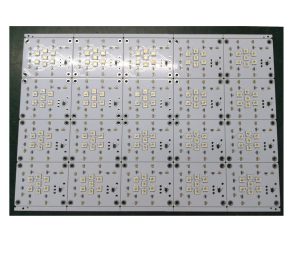
- Lighting: LED driver circuits and illumination products.
- Automotive: Lighting systems, power supplies, and basic control units.
- Medical Devices: Basic diagnostic equipment and monitoring systems.
Conclusion
Single-sided board assembly plays a critical role in the manufacturing of affordable, reliable, and simple PCBs for a variety of applications. Its cost-effective and straightforward nature makes it a preferred choice for many consumer products, automotive systems, and medical devices. While the complexity of PCB designs continues to grow, single-sided assemblies remain a vital part of the PCB manufacturing process, serving as the foundation for many essential electronic devices in today’s world.

- long board pcb
- Flexible PCBs
- Special PCB
- Express Printed Circuit Board
- Pcb Prototype
- LED PCB
- PCB
- Printed Circuit Board
- Pcb meaning
- Pcb manufacturer
- Rigid pcb board
- Rigid Flex PCB
 Quote
Quote
 E-mail