Silkscreen PCB, often referred to as the “marking” layer of printed circuit boards, is a crucial element in the PCB manufacturing process. It serves not only as an essential tool for visual identification but also impacts the functionality and durability of the circuit. In this article, we will delve into the significance of silkscreen PCBs, their manufacturing process, types, benefits, challenges, and the applications across various industries. Let’s uncover what makes silkscreen PCBs a game-changer in electronics.
Silkscreen PCB
1. Introduction to Silkscreen PCB
Silkscreen PCB is a process applied to printed circuit boards where ink is used to mark important components, pads, and other elements on the PCB. It adds the necessary labels and symbols that help in the assembly and identification of the circuit components. What’s the real story? Silkscreen printing isn’t just about marking components—it’s integral to ensuring that the PCB functions properly by providing critical visibility for the assembler.
Silkscreen printing is done using a special type of ink that is applied over the PCB’s copper traces. The main purpose of the silkscreen layer is to indicate where components should be placed, and also to display important circuit information such as part numbers, polarity, and other labeling. Without this step, assembling the PCB would be chaotic and error-prone.
But here’s the kicker: Silkscreen adds both functional and aesthetic value to a PCB. It provides a clear and visible means for assembly teams to quickly identify components, reducing errors and increasing efficiency during the manufacturing process.
Table 1: Key Features of Silkscreen PCB
| Property | Description | Impact on PCB Performance |
|---|---|---|
| Ink Type | Specialized ink used for marking | Ensures clear component identification |
| Durability | Resists wear and damage over time | Increases PCB longevity |
| Visibility | High contrast between components and traces | Enhances assembly speed and accuracy |
| Resistance to Heat | Heat-resistant properties of the silkscreen ink | Prevents damage during soldering and reflow |
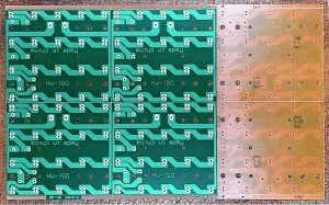
2. What is Silkscreen PCB?
A silkscreen PCB refers to a PCB that has been printed with a layer of ink, which is used for marking essential information about the PCB’s components. The term “silkscreen” comes from the traditional method of printing, where a fine mesh screen is used to transfer ink onto the PCB surface. This layer is primarily used to identify component locations and offer other helpful instructions, such as polarity markings, serial numbers, and other component-related details.
But here’s the kicker: While its primary function is to assist in assembly, the silkscreen layer also contributes to the overall aesthetic and usability of the PCB, which plays a crucial role in user interface and maintenance, especially for end-users or technicians working with the device.
The process of silkscreen printing involves several key steps, from choosing the correct ink type and mesh to carefully printing the desired markings on the surface of the PCB. These marks are usually white or yellow ink, providing high contrast against the copper and making them easy to see.
Table 2: Components of Silkscreen PCB
| Component | Description | Function in the PCB |
|---|---|---|
| Copper Layer | Thin copper traces applied to PCB surface | Carries electrical signals |
| Silkscreen Ink | Special ink used to print markings | Identifies component locations and instructions |
| Substrate | Base material (e.g., FR4) | Provides structural support |
| Soldermask Layer | A protective layer to prevent solder bridges | Prevents electrical shorts and protects traces |
3. The Role of Silkscreen in PCB Manufacturing
Silkscreen plays a critical role in the PCB manufacturing process. It helps mark the component placement and other crucial details that are needed during assembly. Silkscreen is especially important in high-volume manufacturing where precise placement and quick identification are essential. What’s the real story? Silkscreen simplifies assembly and enhances efficiency by ensuring that assembly teams can quickly recognize component locations.
The silkscreen also aids in enhancing the durability and functionality of the PCB. During the soldering process, especially in wave soldering, the silkscreen layer provides a protective layer over the copper traces, preventing them from overheating and maintaining the overall integrity of the PCB. Additionally, the silkscreen ensures that critical components like diodes, capacitors, and ICs are oriented correctly, thus preventing the possibility of incorrect placement.
But here’s the kicker: The silkscreen layer isn’t just a guide for assembly; it plays a vital role in the long-term performance and reliability of the final product.
Table 3: Importance of Silkscreen in PCB Manufacturing
| Benefit | Description | Application |
|---|---|---|
| Component Placement | Identifies the exact location for components | Critical for assembly in mass production |
| Heat Protection | Shields copper traces during soldering | Prevents damage and ensures better soldering |
| Visual Clarity | Enhances visibility of components and traces | Improves the speed and accuracy of assembly |
| Long-Term Durability | Increases the lifespan of the PCB | Provides better overall protection of the board |
4. The Silkscreen Process: How It Works
The silkscreen printing process is a relatively simple yet crucial part of PCB manufacturing. It starts with a photoresist layer on the PCB, where a design is transferred onto the surface using UV light and etching. What’s the real story here? It’s a precise process that requires high accuracy to ensure the component markings are placed correctly and that the quality of the printed text is sharp and readable.
In this process, a mesh screen is used, and the ink is pushed through the mesh and onto the PCB. The ink only passes through the parts of the mesh that are not blocked, leaving behind the desired text or symbols on the board. This process can be done manually or via automated machinery depending on the production scale.
But here’s the kicker: This process ensures that every single board, no matter how small or complex, has consistent and clear markings that are crucial for both assembly and end-use inspection.
Table 4: Steps in Silkscreen PCB Process
| Step | Description | Purpose |
|---|---|---|
| Preparing the Mesh | A fine mesh screen is prepared with the design | Allows ink to be transferred to the PCB |
| Applying the Ink | Ink is pushed through the screen onto the board | Transfers design markings onto the PCB |
| Curing the Ink | The ink is heated to dry and set the printing | Ensures that the ink adheres properly |
| Final Inspection | The silkscreen layer is inspected for defects | Ensures high quality and clarity of markings |
5. Types of Silkscreen Printing Techniques
When it comes to silkscreen PCB printing, there are different techniques that can be employed depending on the scale and complexity of the PCB design. Traditional silkscreen printing, automated printing, and digital printing are the main types used in the industry today.
Traditional silkscreen printing is typically done for small to medium-scale production. It involves manually applying ink to the screen and pressing it onto the PCB, which can be time-consuming but highly effective for custom designs. Automated silkscreen printing, on the other hand, is used for larger volumes and offers increased speed and consistency.
What’s the real story here? As technology advances, digital printing methods are also making their mark in the PCB industry. Digital printing allows for greater flexibility and the ability to print more complex designs without the need for physical screens.
Table 5: Comparison of Silkscreen Printing Techniques
| Printing Technique | Pros | Cons |
|---|---|---|
| Traditional Silkscreen | Cost-effective, highly customizable | Slower and more labor-intensive |
| Automated Silkscreen | Faster, highly consistent, ideal for mass production | Higher initial setup cost |
| Digital Printing | Highly flexible, faster turnaround time | Limited by resolution, not ideal for large volumes |
6. Materials Used in Silkscreen PCB
The quality of a silkscreen PCB heavily depends on the materials used, specifically the ink and the screen mesh. The ink used for silkscreen printing must be capable of withstanding high temperatures and mechanical stress without fading or peeling. Typically, epoxy-based inks are used due to their excellent adhesion properties and durability.
What’s the real story? The type of material chosen for the silkscreen ink directly affects the longevity and readability of the printed markings. In high-performance applications, the silkscreen ink needs to withstand more extreme environmental conditions, which makes material selection a crucial part of the design process.
Another important factor is the choice of the mesh for the screen. Stainless steel or polyester meshes are commonly used for silkscreen printing due to their durability and resistance to wear and tear.
Table 6: Common Materials for Silkscreen Printing
| Material | Properties | Best Use Case |
|---|---|---|
| Epoxy-based Ink | Heat resistant, strong adhesion | High-performance PCBs, automotive electronics |
| Polyester Mesh | Durable, resistant to abrasion | Precision printing for high-density boards |
| Stainless Steel Mesh | Strong, long-lasting | High-volume PCB printing |
7. Key Benefits of Silkscreen PCB
Silkscreen PCB offers numerous benefits that make it the preferred choice for many electronic applications. One of the biggest advantages is the clear visibility of component locations, which helps during the assembly process. This reduces errors and increases manufacturing efficiency.
But here’s the kicker: Silkscreen also helps protect the PCB from environmental factors like moisture and dust, making it a crucial element for enhancing the PCB’s lifespan and functionality.
The ability to clearly mark component polarities, test points, and other key data improves the overall usability of the circuit board. In high-density designs, silkscreen helps prevent mistakes by guiding assembly workers and technicians.
Table 7: Benefits of Silkscreen PCB
| Benefit | Description | Application |
|---|---|---|
| Improved Visibility | Clear marking of components and components placement | Assembly, component identification |
| Enhanced Protection | Shields against external factors like dust and moisture | Industrial, automotive, and medical devices |
| Increased Efficiency | Helps in fast and error-free assembly process | Mass production of PCBs |
8. Common Issues in Silkscreen PCB Printing
Like any manufacturing process, silkscreen PCB printing can encounter a range of issues. Misalignment is one of the most common problems, especially in high-density PCBs where precise placement is crucial. Incorrect ink coverage, smudging, and fading are also frequent issues that can compromise the quality of the final product.
What’s the real story? The silkscreen process is intricate and requires a controlled environment and high attention to detail. Ensuring that all equipment is properly calibrated and that the ink is applied consistently is key to maintaining a high-quality product.
But here’s the kicker: Addressing these issues early in the design and production process can prevent costly errors and delays in the manufacturing process.
Table 8: Common Issues in Silkscreen Printing
| Issue | Cause | Solution |
|---|---|---|
| Misalignment | Incorrect setup or lack of precision | Use automated silkscreen printing techniques |
| Smudging | Excess ink or improper curing | Ensure proper drying and curing processes |
| Fading | Low-quality ink or exposure to high temperatures | Use durable, heat-resistant inks |
9. How Silkscreen PCB Enhances PCB Performance
Silkscreen PCB does more than just mark components; it contributes to the overall performance of the PCB. By ensuring that component placements are correctly identified and by offering protection during assembly, silkscreen layers help maintain the functionality of the circuit board over time.
Ready for the good part? Silkscreen also prevents the occurrence of shorts and misplaced components, which could lead to circuit failure. By providing a clear guide during assembly, the silkscreen layer reduces assembly errors and improves reliability.
Table 9: Silkscreen’s Impact on PCB Performance
| Impact on Performance | Description | Benefit |
|---|---|---|
| Enhanced Assembly | Clear identification of components | Reduces assembly errors, improving efficiency |
| Improved Reliability | Protection during the soldering process | Prevents damage to copper traces and components |
| Increased Longevity | Prevents physical wear and tear | Ensures longer PCB lifespan |
10. Silkscreen PCB for High-Density Circuits
High-density PCBs require precise silkscreen printing to manage the increased number of components and smaller spaces. In these designs, the silkscreen layer must be applied with higher accuracy to prevent errors.
But here’s the kicker: As the complexity of the PCB increases, the silkscreen layer becomes even more critical. Without it, assembly workers could misplace components or fail to follow the correct layout, leading to a non-functional or poorly functioning PCB.
Table 10: Silkscreen’s Role in High-Density PCBs
| Challenge | Solution | Application |
|---|---|---|
| Component Placement | High-precision silkscreen printing | High-density designs like smartphones and tablets |
| Fine Detail | Use of advanced printing technologies | Complex industrial and medical applications |
| Layout Consistency | Automated silkscreen application | High-performance electronic systems |
FAQ Section
Q1: What is silkscreen PCB?
Silkscreen PCB is a printed circuit board with a layer of ink used to mark component placements and other essential details.
Q2: How does silkscreen printing work?
Silkscreen printing involves pushing ink through a mesh screen onto the PCB to create component markings, labels, and instructions.
Q3: What are the benefits of using silkscreen PCBs?
Silkscreen PCBs offer enhanced visibility, better assembly accuracy, and long-term durability by protecting against environmental factors.
Q4: What are common issues in silkscreen PCB printing?
Misalignment, smudging, and fading ink are common problems that can affect the quality of silkscreen printed PCBs.
Q5: How does silkscreen PCB contribute to PCB performance?
Silkscreen PCB helps improve assembly accuracy, prevent errors, and protect the PCB during manufacturing, all of which contribute to overall performance and reliability.

- Flexible PCBs
- Special PCB
- Express Printed Circuit Board
- Pcb Prototype
- LED PCB
- PCB
- Printed Circuit Board
- Pcb meaning
- Pcb manufacturer
- Rigid pcb board
- Rigid Flex PCB
- PCB Board
 Quote
Quote
 E-mail