1. Introduction to Rigid-Flex PCBs
Rigid-Flex PCB Guide: Structure, Benefits, Design & Applications. That’s what we’re here to explore—one of the most advanced and versatile solutions in today’s electronics landscape. Rigid-flex PCBs combine the mechanical stability of rigid boards with the design freedom and flexibility of flex circuits. But here’s the kicker: they’re not just another buzzword in the PCB industry. Rigid-flex PCB technology enables the creation of lightweight, compact, and ultra-reliable electronics—perfect for everything from wearables and medical devices to automotive and aerospace systems. This guide will take you through everything you need to know, including construction, design strategies, material selection, manufacturing, cost considerations, and more. Ready for the good part? Let’s break it down step-by-step and help your business unlock the power of rigid-flex PCB innovation.
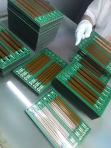
Rigid-Flex PCB
2. Rigid-Flex PCB Structure Explained
The structure of a rigid-flex PCB is where engineering art meets manufacturing science. At the heart of these boards is the hybrid stack-up, blending rigid and flexible layers in a seamless integration. Rigid sections—typically made of FR4—provide sturdy platforms for component mounting, while flexible sections—built from polyimide—offer dynamic bending for folding and complex geometries. But what’s the real story? It’s the ability to route electrical signals through multiple planes and bends, opening up new design frontiers.
Let’s look at key features: the flex layers are usually sandwiched between rigid layers, and copper traces extend continuously through both regions. This integration reduces the need for connectors and cables, slashing points of failure and saving precious space. Electrically, the transition zones between rigid and flex must be carefully engineered to ensure mechanical reliability and signal integrity. Impedance-controlled traces, tailored copper thickness, and specific adhesive systems are often required.
Consider these examples: a medical imaging device that uses a rigid-flex PCB to connect rotating scanner heads with a stationary processing board; a high-end consumer drone with a three-dimensional rigid-flex backbone, reducing assembly weight; or an automotive dashboard controller that combines tactile switches on a rigid panel with flexible links to remote sensors.
| Structure Section | Material | Function | Example |
|---|---|---|---|
| Rigid Layer | FR4 | Mechanical support, components | Control panel |
| Flex Layer | Polyimide | Bendability, dynamic routing | Folding hinge |
| Copper Traces | Copper foil | Signal, power transmission | Data lines |
| Adhesive/Prepreg | Epoxy, acrylic | Bonding, insulation | Layer integration |
| Surface Finish | ENIG, OSP | Solderability, protection | SMD pads |
3. How Rigid-Flex PCBs Work
Ready for the good part? Rigid-flex PCBs work by combining electrical interconnection and mechanical flexibility in a single, integrated package. The copper traces and planes run seamlessly from the rigid sections, through flexible regions, and back again—maintaining signal and power flow even as the flex portions bend, twist, or fold. This isn’t just theory; it’s transformative in practice.
Signal transmission across these areas must account for impedance mismatches, crosstalk, and mechanical strain. Careful design—such as staggered traces and reinforcement at bend points—ensures durability and performance. Component mounting is usually reserved for the rigid zones, where flatness and stability allow reliable soldering of everything from fine-pitch ICs to large connectors. However, passive parts or LEDs can sometimes be found in flex regions for specialized needs.
Power and ground distribution benefit from solid ground planes in the rigid portions, while the flexible areas use carefully designed traces to avoid cracking or metal fatigue over many bend cycles.
Here’s where it gets interesting: a fitness tracker routes data between sensors in the strap and the core unit through a flex region, eliminating bulky cables. A satellite system integrates both rigid control logic and flexible antennas, boosting reliability. And a military headset uses a rigid-flex board for rugged yet ergonomic electronics, withstanding repeated movement in the field.
| Working Principle | Key Aspect | Real-World Example |
|---|---|---|
| Signal Flow | Continuous copper | Wearable sensor |
| Component Mounting | Rigid areas | Smartwatch CPU |
| Flexing/Movement | Dynamic routing | Foldable phone |
| Power/Ground | Shared planes | Avionics board |
4. Types of Rigid-Flex PCBs
Not all rigid-flex PCBs are created equal. The main types include single-sided, double-sided, and multilayer constructions, each serving distinct roles. Single-sided rigid-flex PCBs feature copper on just one side of the flex layer, ideal for basic interconnections or low-profile designs. Double-sided versions increase routing options, allowing for more complex circuits and higher component density.
But here’s where it gets really interesting: multilayer rigid-flex PCBs take complexity to the next level, with alternating rigid and flex layers and multiple copper planes. These are essential for advanced smartphones, medical imaging equipment, or military hardware where size and function cannot be compromised.
Custom stack-ups—combining various thicknesses, controlled impedance layers, or HDI (High Density Interconnect) features—are now possible. Common formats range from simple two-section boards for folding electronics to intricate “origami” designs for space-constrained aerospace modules.
For example, a medical endoscope uses a double-sided rigid-flex PCB for video signal routing. An automotive LIDAR sensor leverages a multilayer stack for robust data processing and power. And a wearable patch uses a single-sided structure for lightweight, flexible operation.
| Rigid-Flex PCB Type | Layer Count | Use Case | Key Feature |
|---|---|---|---|
| Single-Sided | 1 | Basic flex links | Ultra-thin |
| Double-Sided | 2 | Consumer wearables | Higher density |
| Multilayer | 3+ | Smartphones, aerospace | Advanced routing |
| Custom/HDI | Variable | IoT, defense | Miniaturization, reliability |
5. Materials Used in Rigid-Flex PCBs
What’s the real story behind rigid-flex PCB materials? Material selection is absolutely critical for both performance and reliability. The flex layers typically use polyimide, prized for its flexibility, thermal stability, and dielectric properties. For rigid regions, FR4 remains the go-to for its balance of strength, cost, and processability. But that’s just the start.
Copper foils—rolled annealed for flex regions, electrodeposited for rigidity—are chosen to suit dynamic or static requirements. Adhesive systems matter, too: acrylic or epoxy adhesives bond the stack-up, but must withstand repeated flexing without delamination. Solder masks and surface finishes (like ENIG, OSP, or even immersion silver) are applied to protect copper and aid assembly.
Let’s see it in action. A hearing aid uses ultra-thin polyimide and low-profile copper for near-invisible flex circuits. An industrial robot’s rigid-flex board specifies high-Tg FR4 and heavy copper for power delivery. A medical implant opts for medical-grade adhesives and RoHS-compliant finishes for safety and longevity.
But here’s the kicker: the right combination of materials is your best insurance policy for lifecycle durability and field reliability.
| Material | Typical Use | Key Attribute |
|---|---|---|
| Polyimide | Flex sections | Flexibility, heat resistance |
| FR4 | Rigid sections | Mechanical support |
| Rolled Copper | Flex traces | Fatigue resistance |
| Epoxy/Acrylic | Adhesive | Strong bonding |
| ENIG | Surface finish | Solderability, corrosion protection |
6. Rigid-Flex PCB Manufacturing Process
The rigid-flex PCB manufacturing process is a fascinating blend of precision engineering and high-tech craftsmanship. First comes imaging and patterning—photoresist is applied and UV light defines the copper traces on both rigid and flex regions. Etching follows, removing unwanted copper. But here’s where it gets interesting: keeping perfect alignment across rigid and flexible layers is both an art and a science.
Next, micro-drilling creates vias, followed by electroless and electrolytic plating to form interlayer connections. Lamination joins the stack, using heat and pressure to bond rigid and flex materials without causing wrinkles or delamination. The final stages include solder mask and legend printing, surface finishing, electrical testing, and visual inspection.
Real-world cases? A drone manufacturer improved yield by switching to laser direct imaging for intricate flex patterns. A pacemaker OEM doubled reliability with automated AOI and X-ray inspection during final assembly. An avionics supplier reduced field failures by investing in high-pressure, controlled lamination chambers.
Ready for the good part? Rigid-flex PCB production requires strict process control—cutting corners here can compromise your entire product.
| Process Step | Equipment | Critical Control |
|---|---|---|
| Imaging | LDI, UV printer | Alignment |
| Etching | Chemical tanks | Uniformity |
| Drilling | Laser/CNC | Via placement |
| Lamination | Presses, ovens | No delamination |
| AOI/X-ray | Automated | Quality assurance |
7. Rigid-Flex PCB Design Considerations
Designing rigid-flex PCBs is a masterclass in engineering nuance. The first principle? Respect the flex—tight bend radii can crack copper, delaminate adhesives, or stress polyimide. Use generous curves, staggered bends, and reinforced transition zones to extend life. But what’s the real story? Great design starts at the stack-up.
Trace routing matters, too. Keep traces perpendicular to the bend axis, avoid sharp corners, and use fillets or teardrop pads to distribute stress. Controlled impedance, especially in high-speed data lines, requires careful planning of trace width, spacing, and reference planes. DFM (Design for Manufacturability) practices—like standardized via sizes and clear documentation—reduce the risk of costly redesigns.
Consider three cases: a medical device that failed early due to an overlooked bend radius; a consumer wearable that passed 10,000+ flex cycles with properly reinforced traces; an aerospace sensor that minimized signal loss by simulating impedance in the stack-up.
Here’s where it gets interesting: up-front investment in simulation, collaboration with your fabricator, and robust testing pays off every time.
| Design Factor | Impact | Best Practice |
|---|---|---|
| Bend Radius | Flex life | Large, gradual curves |
| Trace Routing | Signal, fatigue | Perpendicular, smooth |
| Impedance Control | Data, RF | Simulate, reference planes |
| DFM | Yield | Standard sizes, clear docs |
8. Key Benefits of Rigid-Flex PCBs
Let’s get right to the point—why choose rigid-flex PCBs? The first and most obvious benefit is space savings. By eliminating connectors, wires, and bulky assemblies, rigid-flex boards shrink device footprints and unlock new design freedom. But here’s the kicker: you also gain reliability by removing potential points of failure.
Weight reduction is another huge win. In wearables, aerospace, and medical devices, every gram counts. Rigid-flex PCBs enable thin, lightweight electronics that don’t sacrifice durability. Complex 3D packaging—think folding phones, modular instruments, or embedded sensors—is now possible.
Case in point: a satellite manufacturer met strict weight targets using rigid-flex. An implantable device passed FDA review by demonstrating lower failure rates versus wired assemblies. And a high-end smartphone used rigid-flex to create a folding hinge with seamless data transfer.
Ready for the good part? These benefits deliver not only better products, but also market differentiation and faster time to market.
| Benefit | Application | Value |
|---|---|---|
| Space Saving | Mobile, medical | Smaller, sleeker |
| Weight Reduction | Aerospace, wearables | Lighter devices |
| Reliability | Automotive, IoT | Fewer failures |
| 3D Packaging | Foldables, modular | Innovative form factors |
9. Limitations and Challenges
Of course, rigid-flex PCBs aren’t all sunshine and roses. Cost is often higher than conventional PCBs, due to complex materials, extra process steps, and intensive inspection. What’s the real story? Sometimes, upfront investment is justified by lower assembly costs and superior performance—but not always.
Manufacturing complexity is a major challenge. Layer alignment, contamination control, and precise lamination all require specialized expertise and equipment. The risk of design errors is higher: a minor mistake in the flex region can lead to costly field failures or recalls.
Case studies abound: a wearable tech startup blew its budget with repeated redesigns; an automotive supplier experienced delamination due to improper lamination settings; a medical device failed certification when transition zones were overstressed.
But here’s the kicker: thorough prototyping, close collaboration with manufacturers, and clear documentation can help manage these risks.
| Challenge | Impact | Mitigation |
|---|---|---|
| Higher Cost | Budget, ROI | Early costing, value analysis |
| Complexity | Process risk | Trusted suppliers, clear specs |
| Durability | Field failures | Prototyping, rigorous testing |
10. Applications of Rigid-Flex PCBs
Rigid-flex PCBs are the unsung heroes behind some of the world’s most innovative devices. Consumer electronics rely on them for foldable smartphones, smartwatches, and VR headsets—products where space, weight, and reliability matter most.
In automotive, rigid-flex PCBs power advanced driver assistance modules, LED lighting arrays, and in-cabin infotainment systems. Aerospace and defense use them for avionics, cockpit controls, and compact sensors, where vibration and movement are constant. Medical applications? Implantable devices, hearing aids, and diagnostic probes are all powered by these hybrid circuits.
But here’s the real story: industrial IoT and robotics use rigid-flex to route signals through moving arms and tight spaces, boosting uptime and performance.
Consider: a sports watch that combines sensor arrays and display in a single assembly; an aircraft cabin panel that withstands repeated cycles; or a surgical tool that meets both miniaturization and sterilization requirements.
| Industry | Example Device | Rigid-Flex Role |
|---|---|---|
| Consumer Electronics | Wearables, phones | Compact, 3D designs |
| Automotive | ADAS, lighting | Durability, reliability |
| Aerospace | Cockpit controls | Flex under vibration |
| Medical | Implants, sensors | Biocompatibility, precision |
11. Quality Standards and Certifications
Quality standards are the unsung heroes of rigid-flex PCB production. IPC-6013 is the global standard for flexible and rigid-flex PCBs, defining everything from material selection to inspection criteria. UL certification is vital for safety in many industries, especially automotive and aerospace.
Testing methods include electrical continuity checks, impedance testing, AOI, and X-ray for hidden defects. Traceability—linking every board to its batch and test record—is critical for medical and defense projects.
Case studies? An avionics supplier gained new contracts by investing in UL and IPC-6013 compliance. A medtech company halved field returns by implementing 100% AOI and serialized tracking. An industrial robotics OEM passed CE certification on the first attempt by prioritizing quality documentation.
What’s the real story? High-quality, standards-compliant rigid-flex PCBs aren’t just about passing tests—they’re your ticket to market and customer trust.
| Standard | Relevance | Required For |
|---|---|---|
| IPC-6013 | Flex/rigid-flex quality | All major markets |
| UL | Safety, flammability | Automotive, aerospace |
| AOI/X-ray | Defect detection | Medical, defense |
| Traceability | Recall, compliance | Medical, industrial |
12. Cost Factors and Quoting
What determines the price tag on a rigid-flex PCB? Materials, process steps, and labor all play a role. Polyimide and high-performance adhesives cost more than standard FR4, and specialized copper foils add further to the bill. Manufacturing complexity—layer count, controlled impedance, and finishing—all add time and resources.
Volume matters, too. Prototypes or small runs are much pricier per unit than large-volume orders. Surface finishes (ENIG, OSP), AOI, and X-ray inspection introduce additional costs but can save money in the long run by catching faults early.
Examples: a wearables startup saved 30% by optimizing layer count and finish selection; an aerospace project paid a premium for full traceability and rigorous inspection; a medical device firm found their ROI justified by avoiding connector failures and streamlining assembly.
But here’s the kicker: clear communication with your fabricator during quoting ensures there are no surprises down the line.
| Cost Factor | Impact | Buyer Strategy |
|---|---|---|
| Material | Major driver | Specify only what’s needed |
| Layer Count | Complexity | Optimize for function |
| Volume | Unit cost | Batch ordering |
| Inspection | Upfront vs. lifecycle | Invest in quality upfront |
13. Innovations and Trends in Rigid-Flex Technology
The rigid-flex PCB world is buzzing with innovation. New materials—ultra-thin polyimides, halogen-free laminates, or embedded shield layers—are opening doors for lighter, safer, and more reliable electronics. 5G integration is driving demand for boards with precise impedance control and low-loss materials.
Miniaturization is a relentless trend: IoT devices and medical wearables demand smaller, thinner, and more robust designs. Rapid prototyping, using digital twins and additive manufacturing, is cutting development cycles and de-risking new projects.
Case in point: a smartphone leader launched a foldable flagship using custom rigid-flex with proprietary shielding. An industrial sensor startup halved development time with in-house rapid prototyping. A medical R&D lab created a biocompatible implant using next-gen adhesives and surface finishes.
Ready for the good part? Staying ahead in rigid-flex means tracking—and investing in—these trends before your competition does.
| Innovation | Advantage | Application |
|---|---|---|
| New Materials | Lighter, safer | Medical, consumer |
| 5G Integration | High-speed data | Telecom, IoT |
| Miniaturization | Compact devices | Wearables, sensors |
| Rapid Prototyping | Faster R&D | Startups, R&D labs |
14. How to Choose a Rigid-Flex PCB Supplier
Choosing the right rigid-flex PCB supplier can make or break your project. Start with technical capability: look for experience, advanced equipment, and a track record in your industry. Certifications—IPC, UL, ISO—aren’t optional; they’re table stakes for quality.
Ask key questions: Can the supplier handle your required volume and complexity? What’s their defect rate, and how do they manage rework or recalls? Strong customer service—prompt communication, engineering support, transparent pricing—sets leaders apart.
Examples: a medtech innovator accelerated to FDA approval by partnering with a supplier who offered on-site design review; an aerospace client avoided costly delays by choosing a manufacturer with global logistics and multi-site redundancy; a robotics firm improved yield by working with a partner invested in continuous improvement and staff training.
Here’s where it gets interesting: treat your supplier as a strategic partner, not just a vendor, and you’ll gain both insight and agility.
| Supplier Factor | Why It Matters | Pro Tip |
|---|---|---|
| Technical Expertise | Complex jobs | Request case studies |
| Certification | Quality, access | Verify credentials |
| Support | Problem-solving | Test responsiveness |
| Flexibility | Growth, risk | Seek multi-site partners |
15. Best Practices for Rigid-Flex PCB Success
Let’s close with some hard-won wisdom. Early collaboration is key—bring your supplier into the design process to catch issues before they become expensive problems. Prototyping and pilot runs are essential for validating both design and process.
Documentation—clear specs, stack-up drawings, test requirements—is your friend. Avoid common pitfalls like ignoring minimum bend radii, over-specifying materials, or skipping reliability testing.
Case examples: an IoT startup hit mass production on schedule after iterative prototyping; a defense project eliminated costly rework with detailed up-front specs; a medical company saved time and cost by using pilot runs to catch rare defects.
But here’s the kicker: the best results come from treating rigid-flex PCB development as a partnership—combining your design goals with your supplier’s process know-how.
| Best Practice | Benefit | Action Step |
|---|---|---|
| Early Collaboration | Fewer surprises | Design reviews |
| Prototyping | Reduced risk | Pilot runs |
| Documentation | Clearer outcomes | Detailed specs |
| Testing | Higher reliability | Lifecycle, fatigue, functional |
Conclusion
Rigid-flex PCBs stand at the frontier of modern electronics, enabling the next generation of compact, lightweight, and reliable devices. Throughout this guide, we’ve examined structure, materials, benefits, design strategies, manufacturing, costs, and innovation trends. The key takeaway? With careful planning, collaboration, and investment in quality, rigid-flex PCBs can give your business the edge in speed, performance, and innovation. Ready to flex your next big idea? Take these lessons, build strong supplier relationships, and lead your industry with confidence.
FAQ
Q1: What is a rigid-flex PCB?
A rigid-flex PCB is a hybrid printed circuit board that combines rigid and flexible layers, allowing complex 3D configurations and reliable connections.
Q2: How does a rigid-flex PCB work?
It transmits signals and power across both rigid and flexible areas, with integrated layers providing electrical and mechanical connectivity.
Q3: What are the main benefits of rigid-flex PCBs?
Benefits include space savings, weight reduction, enhanced reliability, and design flexibility for demanding applications.
Q4: Where are rigid-flex PCBs commonly used?
They are found in wearables, smartphones, medical devices, automotive electronics, and aerospace systems.
Q5: What factors affect rigid-flex PCB cost?
Cost is influenced by materials, layer count, process complexity, order volume, and quality standards.

- long board pcb
- Flexible PCBs
- Special PCB
- Express Printed Circuit Board
- Pcb Prototype
- LED PCB
- PCB
- Printed Circuit Board
- Pcb meaning
- Pcb manufacturer
- Rigid pcb board
- Rigid Flex PCB
 Quote
Quote
 E-mail