Introduction
Printed Circuit Boards (PCBs) are the backbone of modern electronics, providing the necessary infrastructure to connect and power all types of electronic components. As the demand for more compact and high-performance devices increases, PCB designs have evolved to include more advanced features and technologies. One such feature that plays a significant role in enhancing the density and functionality of PCBs is the PHT (Plated Hole Through) via.
In this blog post, we will explore what PHT vias are, their importance in PCB manufacturing, and the impact of PHT vias on the overall PCB quality. We will also discuss the challenges and solutions associated with these vias, and the best practices that manufacturers can adopt to ensure high-quality results.
1. What is a PHT (Plated Hole Through) Via?
A Plated Hole Through (PHT) via is a type of through-hole via that allows for the interconnection of different layers of a PCB through a hole that is drilled through the entire board. After drilling, the via is plated with copper to establish electrical connections between the layers. The term “plated” refers to the process where copper is deposited inside the drilled hole, creating a conductive path from one layer to another.
PHT vias are widely used in both standard PCBs and multi-layer PCBs because they provide an essential method for routing signals and power across different layers. The most common use cases for PHT vias are in high-density interconnects (HDI) and blind or buried vias.
The key distinction of a PHT via from other types of vias is that it is drilled through the entire thickness of the PCB, which makes it highly effective for connecting multiple layers. The plating inside the via helps to form the conductive path, ensuring proper signal transmission.
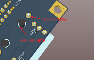
PHT Vias
2. Why Are PHT Vias Important for PCB Manufacturing?
The use of PHT vias in PCB designs is critical for several reasons:
A. Increased Layer Density
As the demand for smaller and more powerful electronic devices grows, PCB designs need to accommodate more functionality within a smaller space. PHT vias are crucial for increasing the number of layers that can be incorporated into a PCB. By allowing for reliable connections between different layers, PHT vias help engineers design multi-layer PCBs that support complex circuits without taking up excessive space.
B. Signal Integrity
Signal integrity is a critical consideration in PCB design, particularly in high-speed circuits or those used in communication devices, such as smartphones, laptops, and networking equipment. PHT vias allow for more effective signal routing between different layers of the PCB, ensuring that signals pass cleanly through the board without loss or interference. Minimizing via resistance and ensuring smooth signal paths are vital for maintaining the performance of high-speed circuits.
C. Cost-Effective Solution
PHT vias offer a cost-effective method for creating multi-layered PCBs compared to other via types, such as blind vias or buried vias, especially when the design requires connections between all layers of the PCB. They are simpler to fabricate and typically do not require the same level of precision or advanced processing techniques as some other via types, making them more affordable for mass production.
D. Structural Integrity
The structural integrity of a PCB is essential, especially in industries that require high reliability, such as aerospace or automotive. PHT vias are crucial for maintaining mechanical strength in a multi-layer PCB, as they help evenly distribute stress across the board. By ensuring that the vias are correctly plated and drilled, manufacturers can prevent issues like delamination and via lifting, which could affect the PCB’s durability and lifespan.
3. Challenges Associated with PHT Vias
Despite their importance in PCB design and manufacturing, PHT vias pose several challenges that can impact PCB quality. Here are the most common issues that manufacturers face:
A. Via Plating Quality
One of the key challenges with PHT vias is ensuring the quality of the plating inside the vias. Uneven plating or insufficient copper thickness can result in poor electrical connections and increased via resistance. Inadequate plating can also cause poor solderability, which can lead to weak solder joints and potential reliability issues. High-quality plating ensures that the via maintains low resistance and a uniform electrical path.
B. Drilling Precision
The drilling process is crucial for ensuring the accuracy and uniformity of the vias. If the hole diameter is too small or irregular, it can affect the plating quality and hinder the PCB’s performance. Excessive drilling speed or worn-out drill bits can lead to poor hole quality, increasing the risk of via wall roughness or misalignment. Inaccurate drilling can cause the vias to be non-circular or lead to uncontrolled via depths, which may affect the overall functionality of the PCB.
C. Thermal and Mechanical Stress
PHT vias are prone to thermal and mechanical stresses during the manufacturing process and under operational conditions. The expansion and contraction of materials during temperature cycling can affect the integrity of the vias. If the vias are not properly plated or if the PCB design does not account for the stresses caused by thermal expansion, delamination or via cracking can occur, leading to reliability issues.
D. Signal Interference and Crosstalk
In high-density designs, PHT vias can introduce issues related to signal interference and crosstalk. When a via is placed too close to high-speed signal traces, the signal integrity can be compromised due to the inductance or parasitic capacitance of the via. The longer the via, the more potential it has to interfere with the signal paths. Reducing via length, minimizing via density, and optimizing via placement can help mitigate this issue.
E. Increased PCB Real Estate Consumption
Although PHT vias are a cost-effective method for creating multi-layer PCBs, they also require more real estate on the PCB compared to other via types. Because PHT vias go through the entire PCB, they can consume valuable space that could otherwise be used for signal routing or additional components. This becomes a problem in high-density designs, where maximizing available space is crucial.
4. The Impact of PHT Vias on PCB Quality
The quality of PHT vias can have a significant impact on the overall quality and reliability of the PCB. Here are some of the major ways in which PHT vias affect PCB quality:
A. Electrical Performance
-
Signal Integrity: The electrical performance of a PCB can be severely impacted if the PHT vias are poorly designed or manufactured. Poor-quality vias can increase resistance, introduce signal degradation, and lead to signal reflections. This is especially problematic in high-frequency applications, where even small imperfections in the via can significantly affect the performance of the circuit.
-
Via Resistance: Insufficient or uneven plating inside the via can increase the resistance of the via, which can, in turn, affect the current flow and overall efficiency of the circuit. For power delivery circuits, higher resistance in vias can cause voltage drops and power loss, leading to overheating and potential failure.
-
Soldering Issues: The quality of PHT vias also affects the soldering process. Poorly plated or improperly drilled vias can lead to cold solder joints, solder bridges, or insufficient solder flow. These issues compromise the mechanical and electrical connection between components and vias, reducing the reliability of the PCB.
B. Mechanical Reliability
-
Via Integrity: In multi-layer PCBs, the mechanical strength of the vias is critical for overall board reliability. If the PHT vias are poorly manufactured, they can lead to stress points in the PCB, causing via lifting, delamination, or cracking over time. This can severely affect the mechanical integrity of the PCB, leading to board failure under thermal cycling, vibration, or physical stress.
-
Fatigue Resistance: PHT vias are subjected to constant stress due to thermal expansion and contraction during normal operation. If not properly designed, the vias can fail over time due to thermal fatigue, leading to cracks or delamination. This is especially problematic in high-reliability applications such as automotive, aerospace, and medical devices, where failure is not an option.
C. Manufacturing Challenges and Yield
-
Increased Rework and Scrap: Poorly manufactured PHT vias can lead to increased scrap rates and rework costs. If the vias do not meet the required standards, they may need to be re-drilled, re-plated, or reworked to meet specifications. This adds to the cost and time required to produce a quality PCB.
-
Throughput Delays: The need for precision drilling and plating processes can slow down production time, particularly for high-density PCBs. In industries with tight deadlines, this can result in delays and missed schedules, affecting time-to-market.
5. How to Improve PHT Via Quality in PCB Manufacturing
To minimize the negative impact of PHT vias on PCB quality, manufacturers can take several steps to improve their design and manufacturing processes:
A. Optimize PCB Design
-
Minimize Via Length: By minimizing the length of PHT vias, designers can reduce their inductive effect and improve signal integrity. This can be achieved by using blind or buried vias where applicable.
-
Optimize Via Placement: Proper placement of vias is essential to avoid interference with high-speed signals. Avoid placing vias directly under critical signal traces or near sensitive components to reduce the risk of signal degradation.
-
Use Via-in-Pad Designs Sparingly: Via-in-pad designs are often used to connect components to internal layers, but they can compromise the solderability and reliability of the PCB. Use this design approach only when absolutely necessary and ensure that the vias are properly plated.
B. Improve Manufacturing Processes
-
Precision Drilling: Using high-quality drills and automated drilling systems can ensure that the vias are drilled accurately and uniformly, minimizing the risk of rough or irregular hole walls.
-
Quality Control for Plating: Ensuring that the plating process is controlled and uniform is essential for the quality of PHT vias. Use pulse plating and other advanced techniques to achieve even copper deposition and minimize defects.
-
Thermal and Mechanical Testing: After the PCB is manufactured, perform thermal cycling and mechanical stress tests to ensure the vias maintain their integrity under different operating conditions.
6. Conclusion
PHT vias are a critical component of modern PCB designs, enabling multi-layer interconnections that are essential for high-performance electronics. However, their quality can significantly impact the electrical performance, mechanical reliability, and overall quality of the PCB. By understanding the challenges associated with PHT vias and adopting best practices in design and manufacturing, PCB manufacturers can improve the performance and reliability of their boards. Ensuring high-quality PHT vias is crucial for creating robust, efficient, and long-lasting PCBs in the competitive electronics market.

- long board pcb
- Flexible PCBs
- Special PCB
- Express Printed Circuit Board
- Pcb Prototype
- LED PCB
- PCB
- Printed Circuit Board
- Pcb meaning
- Pcb manufacturer
- Rigid pcb board
- Rigid Flex PCB
 Quote
Quote
 E-mail