1. Introduction
In the rapidly evolving electronics industry, where precision, miniaturization, and reliability are constantly advancing, the performance of printed circuit boards (PCBs) remains a foundational concern. One recurring issue that can compromise PCB integrity and hinder manufacturing efficiency is PCB warpage. This phenomenon, often underestimated during design or early prototyping stages, can lead to significant functional failures, increased defect rates, and even field returns in finished products.
The challenge of PCB warpage becomes more complex as the demands on circuit boards increase. Multilayered stack-ups, advanced packaging methods like BGA or QFN, high-temperature soldering, and tighter assembly tolerances have all made PCBs more vulnerable to deformation. A slight deviation from flatness can result in uneven solder joints, open circuits, or poor mechanical fit — issues that are difficult to detect but potentially catastrophic for product reliability.
From the perspective of a PCB manufacturer or designer, understanding what causes PCB warpage and how to control it is essential. Warpage is not just a production defect; it’s a systemic problem that spans material selection, stack-up design, thermal processing, handling, and even storage. That’s why addressing PCB warpage requires a multidisciplinary approach, combining engineering knowledge, process discipline, and reliable supply chain practices.
This article provides a comprehensive look into PCB warpage: what it is, why it occurs, and how it can be avoided or corrected. It draws from both theoretical and practical insights, including personal experiences and industry recommendations. Notably, SQ PCB, a leading provider of precision PCB solutions, is highlighted as a reliable partner for warpage prevention, particularly for critical applications where dimensional stability is non-negotiable.
By the end of this article, readers will gain both a technical and practical understanding of how to manage PCB warpage throughout the product life cycle — from concept to mass production.
PCB warpage
2. What Is PCB Warpage?
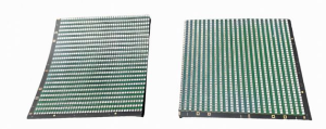
PCB warpage is defined as the undesired deformation of a printed circuit board from its original flat plane. Ideally, a PCB should be perfectly flat, allowing it to sit evenly on the assembly platform and align properly with components and connectors. However, due to internal stresses or environmental effects, the board may warp into different shapes: commonly bow (concave or convex) or twist (diagonal deformation).
2.1 Common Forms of PCB Warpage
-
Bow (bending along length/width): The entire board curves upward or downward, forming an arc.
-
Twist (diagonal warping): Opposite corners of the board are displaced vertically, resulting in a “potato chip” shape.
-
Dome or Saddle Warpage: Often seen in large boards, where the center bulges outward or inward while corners remain flat.
While minor warpage might not affect all assemblies, any deviation that exceeds acceptable IPC standards (e.g., 0.75% for surface-mount boards) can result in misalignment, improper soldering, or mechanical stress on components.
2.2 How Warpage Affects Manufacturing and Product Reliability
-
Solder Joint Failure: Uneven contact between components and pads during reflow can cause cold solder joints or opens.
-
Automated Assembly Issues: Pick-and-place machines require flat surfaces to correctly place components.
-
Mechanical Assembly Constraints: Warped boards may not fit within tight mechanical enclosures.
-
Signal Integrity Loss: Excessive flexing or strain can impact trace impedance and high-speed signal paths.
-
Stress on Components: Large packages (e.g., BGA) are particularly sensitive to warpage-induced stress during solder reflow.
In my experience, even small-scale projects are not immune to these issues. One prototype batch I worked on exhibited a 0.9% bow due to an unbalanced copper layer in a four-layer board. Despite appearing minor, it caused intermittent connectivity on the QFN pins, delaying the product’s validation phase by two weeks.
2.3 Key Causes Behind PCB Warpage
Understanding what causes PCB warpage is crucial to mitigating it. Warpage usually results from internal stress imbalance, introduced during different stages of the PCB lifecycle:
-
Material Mismatch: Different materials in the PCB (copper, FR4, resin) expand and contract at different rates under heat.
-
Asymmetric Stack-ups: If the layer arrangement is not symmetrical, thermal expansion causes one side to pull more than the other.
-
High Temperature Reflow: Heating during soldering can exaggerate internal stresses or moisture vaporization.
-
Moisture Absorption: PCBs stored improperly may absorb humidity, which turns into vapor and causes expansion during reflow.
-
Mechanical Handling: Bending or twisting during assembly, especially when boards are thin or unsupported, adds stress.
-
Improper Storage: Warpage can occur when boards are stored on uneven surfaces, under weight, or without ESD-safe conditions.
These contributors may occur singly or in combination, making warpage a cumulative problem. The earlier it’s detected — during incoming inspection or prototyping — the better the chances of preventing mass production defects.
3. Identifying and Measuring PCB Warpage
Before a PCB warpage issue can be resolved, it must first be accurately identified and quantified. Detecting warpage early—preferably before the assembly stage—saves both time and cost. In practice, identifying PCB warpage requires more than visual inspection; it often involves precision measurement tools and adherence to international standards.
This section discusses how to properly inspect, measure, and evaluate PCB warpage, with insights into both manual and automated techniques used in prototype and high-volume production.
3.1 Why Measuring PCB Warpage Matters
PCB warpage, when undetected, can cause subtle failures that are difficult to trace back during functional testing. A warped PCB may pass initial electrical tests but fail in dynamic conditions like thermal cycling, vibration, or during surface-mount component soldering.
In automated assembly lines, even slight PCB warpage may prevent successful component placement or reflow soldering. This is particularly relevant for Ball Grid Array (BGA), Quad Flat No-lead (QFN), or Chip Scale Package (CSP) components, which require precise coplanarity. Ensuring the PCB meets flatness requirements protects against yield loss and quality escapes.
3.2 Industry Standards for PCB Warpage Tolerance
The IPC-A-600 and IPC-6012 standards provide guidelines on acceptable levels of PCB warpage:
-
For PCBs without surface mount devices (SMD):
≤1.5% of the PCB diagonal length. -
For PCBs with SMDs:
≤0.75% of the PCB diagonal length.
These tolerances are calculated as the maximum bow or twist divided by the diagonal dimension of the board. Any deviation beyond these values requires corrective action or rejection.
Let’s take an example: For a 150 mm × 100 mm PCB (diagonal ≈ 180 mm), the maximum allowable warpage for an SMD board would be:
0.75% × 180 mm = 1.35 mm
If warpage exceeds 1.35 mm, the board is non-conforming per IPC standards.
3.3 Visual Inspection and Preliminary Identification
Basic visual inspection remains a useful first step, especially for small batch runs or prototypes:
-
Flat Table Test: Place the PCB on a known flat granite or glass surface and observe if any corners lift or if there’s rocking movement.
-
Light Gap Check: Shine a backlight under the PCB. Any light leakage indicates deviation from flatness.
-
Manual Twist Test: Gently press diagonally opposite corners of the board. Excessive flexing may signal warp or twist.
Although these methods are low-tech, they can quickly flag boards for further inspection without requiring special equipment.
3.4 Measurement Tools for PCB Warpage
To quantify warpage and comply with IPC standards, precise measurement is necessary. Here are commonly used tools and methods:
a. Dial Gauge and Fixture Method
-
A dial indicator mounted on a movable arm measures the height difference at specific board locations.
-
The PCB is placed on support pins or a vacuum fixture to simulate the assembly platform.
-
Measurements are taken at the four corners and the center.
-
This method is low-cost but requires skilled technicians for repeatability.
b. Laser Displacement Sensors
-
Laser sensors scan the surface of the PCB and measure distance to the reference plane.
-
These are highly accurate and suitable for both flatness and twist measurements.
-
Results can be exported for statistical analysis.
c. 3D Optical Inspection Systems
-
Used in automated optical inspection (AOI) stations or dedicated warpage measurement platforms.
-
Capture millions of data points to generate a 3D surface map of the PCB.
-
Useful for capturing local deformations and warpage trends over time.
-
Common in high-reliability industries such as aerospace, automotive, and medical electronics.
d. Shadow Moiré System
-
This advanced system uses light patterns and interference imaging to detect warpage.
-
Highly sensitive and accurate.
-
Often used for small, high-density PCBs or in R&D labs.
3.5 Real-World Warpage Analysis: A Case Study
In a recent project for an automotive customer, our team at a contract manufacturing facility observed high defect rates during QFN soldering. Visual inspections showed minor coplanarity issues, but AOI flagged hundreds of failures. We employed a 3D warpage scanner and found that the PCB warpage reached 1.7 mm on a 200 mm diagonal — well above IPC tolerance.
Root cause analysis traced the issue to unbalanced copper distribution across layers and improper bake prior to reflow. Post-revision, with help from suppliers like SQ PCB who implemented a symmetric stack-up and enforced pre-bake routines, the problem was eliminated, and yields improved from 88% to 99.5%.
3.6 Using Data to Monitor and Prevent PCB Warpage
Measurement alone isn’t enough; the data collected from warpage analysis should feed back into process control. Manufacturers and engineers should:
-
Maintain SPC charts for warpage over time.
-
Analyze warpage by panel, batch, or material supplier.
-
Link warpage measurements with process parameters (e.g., lamination cycle, copper thickness).
-
Set preventive thresholds to catch deviations before reaching IPC limits.
This data-driven approach allows for continuous improvement, early defect prediction, and overall reliability enhancement.
3.7 Recommendations for Effective PCB Warpage Detection
-
For prototypes or small runs: Use dial indicators or flat-surface inspection with visual aids.
-
For medium to high-volume runs: Implement 3D scanning systems or integrate warpage tests into AOI stations.
-
Establish a pre-reflow warpage check as part of quality inspection.
-
Consider working with experienced manufacturers such as SQ PCB, who offer advanced in-house testing and process validation for PCB warpage control.
4. Major Factors Causing PCB Warpage
Understanding the root causes behind PCB Warpage is essential for any manufacturer, designer, or quality engineer. Warpage rarely stems from a single factor; rather, it is the result of a complex interplay of material characteristics, process parameters, environmental conditions, and design choices. This section breaks down the primary contributors to PCB Warpage and offers technical insights into how each factor contributes to dimensional instability.
4.1 Material Selection and PCB Warpage
The materials used in PCB fabrication significantly influence PCB Warpage behavior under thermal and mechanical stress.
a. Dielectric Substrate (FR4 and Alternatives)
Standard FR4 materials have a coefficient of thermal expansion (CTE) around 13–17 ppm/°C in the X/Y axis and up to 70 ppm/°C in the Z-axis. This mismatch between layers—especially during heating—can cause internal stress and warping. High-Tg or low-CTE materials such as polyimide or ceramic-filled laminates can reduce this risk.
b. Copper Distribution
Uneven copper distribution leads to asymmetric thermal expansion. A board with heavy copper fill on one side and sparse traces on the other will expand unevenly, causing curvature under heat.
c. Prepregs and Cores
Using dissimilar prepregs or mixing resin systems (e.g., halogen-free and standard) may introduce mechanical mismatch. Selecting prepregs with similar Tg and modulus values across layers helps maintain mechanical equilibrium.
Tip: Manufacturers like SQ PCB offer material consultation services that help select balanced, low-warpage materials suitable for high-layer count or thermally demanding applications.
4.2 Layer Stack-up Design and PCB Warpage
A poorly planned stack-up is a common but often overlooked cause of PCB Warpage.
a. Asymmetrical Layer Arrangement
If the copper and dielectric layers are not mirrored around the center plane, the board will bend toward the side with greater mass or copper density during heating or cooling.
b. Non-uniform Dielectric Thickness
Varying thickness between layers (e.g., using thicker cores on one side) disturbs stress balance during lamination and soldering.
c. Ground/Power Plane Imbalance
Ground and power planes should be symmetrically placed. An offset in these planes can shift the neutral axis of the board, amplifying warpage effects.
d. Copper Pour Strategy
Leaving large unconnected copper pours on one side while the other has routed traces is a recipe for localized warpage during reflow.
Best Practices to Avoid Stack-up Related Warpage:
-
Use symmetrical construction with mirrored layers.
-
Distribute copper evenly or use copper balancing.
-
Avoid “floating” copper zones without thermal relief.
-
Verify stack-up with FEA (Finite Element Analysis) tools during design.
4.3 Thermal Processing and PCB Warpage
Temperature is one of the most influential factors affecting PCB Warpage during manufacturing and assembly.
a. Lamination Process
During multilayer lamination, improper heat ramp-up or insufficient pressure uniformity causes layer misalignment or inner layer stress. Non-uniform heating may leave residual stresses that manifest as warpage post-cooling.
b. Reflow Soldering
Reflow profiles directly affect PCB behavior. Rapid heating, uneven top/bottom surface temperature, or uncontrolled cooling often trigger PCB Warpage. Boards with heavy copper content require slower temperature ramps to ensure uniform expansion.
c. Wave Soldering (for through-hole)
Longer exposure to high heat in wave soldering can cause thin or asymmetric boards to deform, especially if unsupported.
4.4 Moisture Absorption and PCB Warpage
Moisture is a silent but serious contributor to PCB Warpage.
PCBs are hygroscopic by nature, especially FR4-based boards. When boards absorb moisture during storage or transit and are then exposed to reflow soldering, rapid steam expansion within the layers can cause blistering or board bending.
Risk Indicators:
-
Improper packaging (non-vacuum sealed or desiccant expired)
-
Storage in high-humidity environments
-
Long shelf life (>6 months without rebake)
Preventive Measures:
-
Bake PCBs at 120°C–125°C for 4–12 hours before reflow if moisture is suspected.
-
Vacuum seal boards with desiccants immediately after fabrication.
-
Use dry cabinets for storage (humidity <5% RH).
SQ PCB, for instance, includes dry packaging and pre-bake options as standard in their export protocol, helping customers avoid moisture-induced PCB warpage before final assembly.
4.5 Mechanical Handling and PCB Warpage
Physical handling and storage procedures can also trigger or exacerbate PCB Warpage.
Common Handling Mistakes:
-
Stacking boards unevenly or with overhang
-
Placing heavy objects on board stacks
-
Transporting boards without mechanical support
-
Inserting/removing boards from test fixtures by force
Recommendations:
-
Always store PCBs flat on a stable, level surface.
-
Use rigid carriers during transportation or reflow.
-
Train assembly personnel to handle boards by the edges.
-
For thin or high-layer-count PCBs, use vacuum fixtures or aluminum stiffeners during assembly.
4.6 Combined Effects and System-Level PCB Warpage
Often, PCB Warpage is the result of multiple overlapping factors. A board may have perfect symmetry but still warp due to a combination of marginal material choice and insufficient moisture control. Conversely, robust materials may still warp if stack-up design is careless.
Understanding this interaction requires cross-functional collaboration between PCB designers, fabricators, and assemblers. Running Design of Experiments (DOE) during prototyping can help isolate contributing factors and develop mitigation strategies before scaling to volume.
5. How to Avoid PCB Warpage
Preventing PCB Warpage requires a holistic approach that spans the entire PCB lifecycle — from design and material selection to thermal processing, handling, and storage. While some degree of board deformation may be inevitable due to the physical characteristics of multilayer materials, the goal is to keep the warpage within acceptable IPC tolerances and ensure functional reliability during assembly and field use.
This section presents practical, actionable methods to minimize the risk of PCB Warpage, based on industry best practices, root cause analysis data, and real-world case experiences.
5.1 Material Strategy to Avoid PCB Warpage
Choosing the right materials is the first and most foundational step in warpage prevention.
a. Use Low-CTE Laminates
-
Choose base materials with low and uniform coefficients of thermal expansion (CTE).
-
High-Tg FR4, polyimide, or ceramic-filled resins are more dimensionally stable under heat and moisture exposure.
-
Avoid mixing incompatible resin systems in the same stack-up.
b. Balance Copper Types and Weights
-
Use consistent copper thickness across layers to maintain thermal symmetry.
-
Employ copper balancing techniques on signal layers to minimize expansion mismatch.
c. Select Quality Vias and Fill Materials
-
Resin-filled vias with low shrinkage properties help maintain structural integrity.
-
Avoid poorly cured fill materials which may shrink unevenly during heating.
5.2 Optimized Stack-Up Design to Prevent PCB Warpage
A well-structured layer stack is the second line of defense against PCB Warpage.
a. Ensure Stack Symmetry
-
Design copper and dielectric layers in a mirrored fashion across the PCB center axis.
-
Avoid uneven trace density or isolated plane layers on one side.
b. Use Balanced Core and Prepreg Combinations
-
Maintain consistent dielectric thickness between layers.
-
Avoid stacking all thicker materials on one side of the board.
c. Account for Finished Copper Distribution
-
During the layout stage, use copper balancing fill patterns in sparse regions to match density on both sides.
-
Avoid excessive copper near one edge of the PCB.
d. Simulate Warpage Early
-
Use design tools with FEA simulation to anticipate thermal stress behavior in the chosen stack-up.
-
Collaborate with fabricators early in the design process to validate mechanical symmetry.
5.3 Thermal Process Control to Limit PCB Warpage
Thermal treatment during both fabrication and assembly plays a critical role in PCB Warpage mitigation.
a. Lamination Process Control
-
Apply uniform pressure and temperature during lamination to avoid internal layer shifting or trapped stresses.
-
Allow gradual cooling under pressure to minimize post-process relaxation.
b. Reflow Profile Optimization
-
Use a ramp-soak-spike reflow profile tailored to the board’s copper loading and laminate characteristics.
-
Minimize top-to-bottom temperature differential.
-
Avoid rapid heating or cooling that can induce flexing.
c. Multiple Reflow Considerations
-
For double-sided assemblies, design components and profiles so the first side remains within thermal tolerance during second reflow.
🔧 Tip: Collaborating with your assembly partner to design reflow profiles specific to the board type and stack-up is crucial. SQ PCB, for instance, offers pre-profile testing and simulation services that minimize risk during reflow.
5.4 Moisture Control to Avoid PCB Warpage
Moisture management is often overlooked, yet it plays a significant role in board deformation.
a. Store PCBs in Dry Environments
-
Use moisture barrier bags (MBB) with desiccants.
-
Place humidity indicator cards (HIC) inside each package.
-
Keep boards in a dry cabinet (<5% RH) if opened.
b. Pre-Bake Before Reflow
-
Bake boards at 120–125°C for 4–12 hours, depending on thickness and storage conditions.
-
Pre-baking removes absorbed moisture and reduces risk of internal delamination or board warping.
c. Control Humidity During Fabrication
-
Monitor humidity in lamination, drilling, and surface finish areas.
-
Apply humidity alarms in storage areas.
5.5 Mechanical Support and Handling Best Practices
Even with optimal materials and thermal profiles, poor handling can introduce or worsen PCB Warpage.
a. Use Rigid Fixtures or Carriers
-
Thin or large-format PCBs should be placed on aluminum or ceramic carriers during reflow and transport.
-
Carriers prevent gravity-induced sagging and maintain flatness.
b. Avoid Overstacking or Hanging
-
Stack PCBs horizontally and evenly with flat interlayers.
-
Avoid vertical stacking unless using board clamps or edge supports.
c. Train Personnel for Proper Handling
-
Educate operators on ESD-safe and warp-minimizing techniques.
-
Avoid bending, flexing, or pressing boards during inspection or test.
d. Monitor and Minimize Residual Stress
-
Review placement tooling and test fixtures to ensure no excessive force is applied.
-
For high-layer-count boards, consider post-lamination flattening under uniform weight for 24 hours.
5.6 Design-for-Manufacturability (DFM) Measures
By embedding warpage prevention into the design stage, many downstream issues can be avoided.
-
Collaborate early with your PCB manufacturer to validate stack-up structure.
-
Incorporate copper balancing and pre-layout constraints.
-
Use DFM checks for copper density, hole spacing, and thermal profiles.
-
Specify board flatness tolerances on fabrication drawings.
6. Dealing With PCB Warpage in Prototypes and Mass Production
While preventing PCB Warpage is critical during the design and fabrication phases, the real challenge lies in how to manage it when it arises in both prototype and mass production environments. Warpage can emerge in a prototype due to early process optimization issues or in mass production due to variations in material consistency, process conditions, or unforeseen environmental factors. In either case, it’s crucial to quickly identify the problem, analyze its root cause, and implement effective corrective actions.
This section outlines effective strategies for handling PCB Warpage at two critical stages: the prototype phase and mass production.
6.1 Managing PCB Warpage in Prototypes
Prototypes are often the first place where warpage issues surface, mainly due to the relatively high degree of experimentation with materials, stack-up designs, and processing conditions. In the prototype stage, there are often unknowns that haven’t been fully explored, such as material interactions or thermal profiles.
a. Early Detection in Prototypes
-
Visual Inspection: Although not the most precise method, visual inspection should always be the first step. Look for signs of bowing or twisting by placing the board on a flat surface or using light gap checks.
-
Dimensional Measurement: Use dial indicators or simple tools like micrometers to measure the height difference between corners. This helps quickly quantify warpage.
-
AOI (Automated Optical Inspection): While AOI is typically used for quality control after assembly, it can also detect warped or misaligned boards in the prototype stage, flagging any dimensional issues before they affect assembly.
b. Revising the Design and Stack-up
Once PCB Warpage has been detected in prototypes, it’s essential to iterate on the design. In this phase, any detected warpage can often be traced back to issues with material choice or stack-up asymmetry.
-
Symmetry Adjustments: Adjust the layer stack to ensure symmetry, especially in multi-layer PCBs. Ensure copper balance on both sides of the board, and review prepreg thickness across layers.
-
Material Tweaks: Swap out the existing material for lower CTE options (e.g., high-Tg materials) to mitigate thermal expansion issues.
-
Prototype Testing: After modifications, run additional testing with the updated designs. Use warpage measurement tools, such as laser displacement sensors or 3D scanners, to ensure the corrected design is within IPC tolerance.
Recommendation 1: SQ PCB offers dedicated prototyping services with real-time monitoring for warpage and other dimensional defects. Their comprehensive testing ensures early identification of warpage issues, allowing designers to refine prototypes before moving to mass production.
c. Post-Rework Options
If warpage is still present in the prototype after adjustments, consider reworking the board. Here are a few rework options:
-
Reflow and Flattening: For minor warpage, a reflow cycle with an adjusted thermal profile may help flatten the board, especially for smaller designs.
-
Post-Lamination Flattening: For multi-layer boards, applying pressure and uniform heat post-lamination can help reduce warp.
6.2 Dealing with PCB Warpage in Mass Production
Once a design transitions from prototype to mass production, controlling PCB Warpage becomes even more critical. While prototype runs allow for flexibility and design adjustments, mass production requires a much more standardized and disciplined approach.
a. Warpage Monitoring in Mass Production
-
Statistical Process Control (SPC): Implement SPC charts to track warpage measurements across different batches. Regularly monitor the bow and twist values of a sample from each production lot. If the values exceed acceptable limits, corrective actions can be taken proactively.
-
In-Line Inspection: Incorporate warpage measurement into the production line at multiple stages: after PCB fabrication, after assembly, and post-reflow. Using automated measurement systems such as 3D scanners or laser displacement sensors can help continuously monitor and catch issues early.
-
Root Cause Analysis: If warpage exceeds tolerance limits, perform root cause analysis. Possible causes in mass production include material batch variations, inconsistent lamination pressure, or irregular reflow profiles.
b. Batch Process Control
-
Material Lot Tracking: Ensure that materials (e.g., prepreg, copper) are batch-controlled. Inconsistent material lots can lead to variations in board properties, contributing to warpage. When problems are traced to a specific batch, it’s easier to isolate the cause and remedy it.
-
Thermal Profile Consistency: Recheck and calibrate your reflow oven periodically to ensure that heat distribution is uniform. Small temperature variations across the oven zones can cause uneven expansion during reflow, leading to warpage.
-
Pressure Control During Lamination: Even minor changes in the pressure during lamination can result in warpage. Consistently check lamination pressure and temperature profiles to ensure uniform conditions.
-
Pre-bake Moisture Control: Ensure that moisture levels are controlled in mass production. Implement routine pre-baking for PCBs, especially those that have been stored for extended periods or are at higher risk of moisture absorption.
c. Adjusting Post-Production for Warped Boards
-
Manual Flattening: For minor warpage in mass production, you can use manual flattening techniques. This involves applying slight pressure or heat to flatten the board, especially for smaller batches.
-
Reflow Rework: Boards with minor warpage can sometimes be reworked in the reflow oven by adjusting the profile to focus more heat on areas that need flattening.
-
Post-Assembly Fixturing: After assembly, if warpage is found, use mechanical fixturing or specialized fixtures during the soldering process to hold the board flat and minimize further distortion during solder cooling.
Recommendation 2: SQ PCB ensures that their mass production lines include strict in-line quality control for warpage and dimensional accuracy. Their dedicated monitoring systems help prevent production delays, minimizing defect rates and maintaining consistent product quality.
6.3 Warpage Handling Best Practices
To handle PCB Warpage in both prototypes and mass production effectively, manufacturers must follow a systematic approach:
-
Design Validation: Use advanced simulation tools during the design phase to predict and mitigate potential warpage issues.
-
Early Detection: Implement early and rigorous warpage testing, especially for critical applications such as high-frequency or high-reliability boards.
-
Collaborate with Trusted Suppliers: Work with trusted PCB fabricators like SQ PCB to ensure high-quality material choices and accurate stack-up designs from the outset.
-
Continuous Improvement: Establish a feedback loop from production to design, ensuring that any warpage issues encountered in mass production are systematically fed back to the design team for review and improvement.
6.4 Conclusion: Addressing Warpage in Production Stages
Dealing with PCB Warpage is a continuous effort that spans multiple stages of the PCB lifecycle, from design through mass production. While prototype runs allow for more flexibility in correcting issues, mass production requires more stringent controls and monitoring systems to prevent warpage. By implementing precise inspection, process control, and material management strategies, manufacturers can mitigate the impact of warpage, improving yields and ensuring the reliability of end products.
With the right approach and partnerships—like those offered by SQ PCB—you can reduce the risk of PCB Warpage in both prototypes and high-volume production, ensuring a higher yield and better product quality.
FAQ: Common Questions About PCB Warpage and Related Topics
This final section addresses some of the most frequently asked questions engineers, designers, and purchasers have regarding PCB Warpage and related manufacturing concepts. The answers below are based on best practices in the industry and hands-on experience from both prototyping and large-scale PCB manufacturing.
-
What is the difference between rolled copper foil and electrolytic copper foil?
Rolled copper foil is produced by mechanically rolling copper into thin sheets, offering better surface quality and mechanical strength. Electrolytic copper foil is deposited via an electrolytic process and is more flexible and cost-effective. -
Can mechanical warpage be fixed after production?
Minor warpage can be corrected by reflow over flat vacuum fixtures, but major warpage usually requires redesign or remanufacture. -
How does board thickness affect warpage?
Thicker boards are generally stiffer and less prone to warpage, but they may exacerbate warp if layer stresses are unbalanced. -
Is moisture the biggest warpage culprit in mass PCB runs?
Yes, moisture absorption significantly increases warpage during reflow. Proper drying and moisture control are vital. -
What inspection tools detect PCB Warpage quickly in production?
3D optical scanners or curvature gauges can quickly flag warpage beyond tolerance before assembly.

- long board pcb
- Flexible PCBs
- Special PCB
- Express Printed Circuit Board
- Pcb Prototype
- LED PCB
- PCB
- Printed Circuit Board
- Pcb meaning
- Pcb manufacturer
- Rigid pcb board
- Rigid Flex PCB
 Quote
Quote
 E-mail