Introduction
Printed circuit board (PCB) warpage is a significant issue in the electronics industry, affecting product reliability, assembly precision, and long-term performance. As modern electronic devices continue to demand higher precision and smaller form factors, the importance of controlling PCB warpage has become paramount. This article explores PCB warpage in depth, covering its causes, effects, mitigation strategies, case studies, and future trends.
1. Understanding PCB Warpage
What Is PCB Warpage?
PCB warpage refers to the unwanted bending or deformation of a PCB, typically occurring during the manufacturing or assembly process. Warpage can lead to assembly misalignment, poor soldering quality, and failures in electronic components.
Types of PCB Warpage
- Global Warpage: The entire PCB deforms in a curved shape due to thermal expansion, mechanical stress, or material mismatches.
- Local Warpage: Warpage occurs in specific areas of the PCB, often around high-density component regions or uneven copper distribution.
- Twisting and Bowing: The PCB may twist along its diagonal axis (twisting) or form a convex or concave shape (bowing).
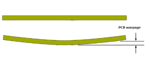
PCB warpage
2. Causes of PCB Warpage
Material-Related Causes
- Coefficient of Thermal Expansion (CTE) Mismatch: Different PCB materials expand and contract at varying rates under temperature changes, leading to stress accumulation.
- Moisture Absorption: PCBs absorb moisture from the environment, which expands when exposed to heat, causing warpage.
- Uneven Copper Distribution: High copper content on one side of the PCB creates an imbalance in thermal expansion, leading to warpage.
Manufacturing-Related Causes
- Lamination Process Issues: Uneven pressure or improper temperature control during lamination can cause internal stress, leading to warpage.
- Improper Layer Stack-Up: Asymmetrical PCB layer structures result in imbalanced stress distribution, increasing the risk of warpage.
- Excessive Panel Size: Large PCB panels are more prone to warpage due to their increased exposure to thermal stress and mechanical forces.
Assembly-Related Causes
- Reflow Soldering Heat Stress: During reflow soldering, uneven heat distribution can cause differential expansion and lead to PCB warpage.
- Component Placement and Weight Distribution: Heavy components placed asymmetrically can introduce stress points, increasing the risk of localized warpage.
- Improper Cooling Process: Rapid cooling after soldering can create thermal shock, which increases the likelihood of PCB deformation.
3. Effects of PCB Warpage on Manufacturing and Performance
Impact on Assembly Process
- Solder Joint Defects: Warpage can lead to poor contact between components and solder joints, increasing the risk of cold joints or solder bridging.
- Component Misalignment: If the PCB does not sit flat on the assembly fixture, components may be misplaced, affecting the functionality of the final product.
- Reduced Yield Rates: Higher warpage levels result in more defective boards, leading to increased scrap rates and manufacturing costs.
Impact on Product Performance
- Signal Integrity Issues: Warped PCBs can cause variations in trace geometry, impacting high-speed signal transmission.
- Mechanical Stress on Components: Warpage can exert excessive mechanical force on soldered components, leading to premature failures.
- Reliability Concerns: Long-term exposure to thermal cycling can exacerbate warpage-related defects, reducing the lifespan of electronic devices.
4. Strategies to Mitigate PCB Warpage
Material Selection Strategies
- Choose Low-CTE Materials: Opt for PCB laminates with a low coefficient of thermal expansion, such as high-Tg FR-4 or polyimide-based substrates.
- Use Moisture-Resistant Laminates: Materials with low hygroscopic properties help reduce warpage caused by moisture absorption.
- Optimize Copper Distribution: Ensure even copper distribution across PCB layers to balance thermal expansion forces.
Manufacturing Process Improvements
- Symmetrical Layer Stack-Up Design: Designing PCB layers in a symmetrical manner helps distribute stress evenly, reducing the risk of warpage.
- Controlled Lamination Pressure and Temperature: Optimizing lamination conditions ensures uniform bonding and minimizes internal stress buildup.
- Reduce Panel Size for Large PCBs: Using smaller panels or designing break-off sections can help manage warpage in large PCBs.
Assembly Process Optimizations
- Gradual Heating and Cooling in Reflow Soldering: Implementing controlled heating and cooling profiles minimizes thermal shock and prevents warpage.
- Component Weight Balancing: Distributing heavy components evenly across the PCB reduces mechanical stress on specific areas.
- Use of PCB Fixtures During Assembly: Holding the PCB in place using fixtures or stiffeners during reflow soldering prevents excessive deformation.
5. Case Studies on PCB Warpage
Case Study 1: Warpage in High-Frequency PCBs
A telecommunications company faced severe PCB warpage issues in high-frequency circuit boards. The use of PTFE-based laminates caused CTE mismatches, leading to misalignment during assembly. By switching to a hybrid stack-up with reinforced glass fiber layers, they significantly reduced warpage and improved yield rates.
Case Study 2: Warpage in Multilayer PCBs
An automotive electronics manufacturer experienced warpage in a 12-layer PCB design. Asymmetrical copper distribution and excessive lamination pressure led to defects. By redesigning the PCB stack-up and optimizing the lamination process, they reduced warpage by 60%.
6. Future Trends in PCB Warpage Management
Advanced Materials Development
New PCB materials, such as ultra-low-CTE laminates and moisture-resistant substrates, are being developed to address warpage challenges. These materials offer improved dimensional stability and thermal performance.
AI-Driven Process Control
Artificial intelligence and machine learning algorithms are being integrated into PCB manufacturing to predict and control warpage in real time. AI-based monitoring systems can adjust process parameters dynamically to minimize defects.
Flexible and Rigid-Flex PCBs
Flexible and rigid-flex PCBs are gaining popularity due to their ability to absorb mechanical stress, reducing warpage risks in applications requiring high reliability.
3D-Printed PCBs
3D-printed PCB technology is emerging as a potential solution for warpage management. By precisely controlling material deposition and curing processes, manufacturers can minimize stress buildup and improve PCB flatness.
7. Advanced Strategies to Further Reduce PCB Warpage
As PCB designs become more complex, controlling PCB warpage requires a multi-faceted approach. Beyond standard material selection and manufacturing process improvements, advanced techniques and technologies can significantly minimize warpage and improve production yield.
7.1 Optimizing PCB Layout for Warpage Prevention
Balanced Copper Distribution
Copper density differences between PCB layers can cause thermal stress during the lamination and soldering processes, leading to warpage. To mitigate this:
- Ensure that each PCB layer has an even copper distribution to balance heat dissipation.
- Use cross-hatching patterns in copper pours instead of solid copper planes to reduce stress differentials.
- Avoid large unconnected copper areas that may expand unevenly during reflow soldering.
Minimizing PCB Aspect Ratio Issues
The aspect ratio (length-to-width ratio) of a PCB panel significantly impacts its tendency to warp. Strategies to reduce warpage include:
- Keeping the aspect ratio below 4:1 to minimize mechanical stress accumulation.
- Using fiducial markers and support structures to prevent excessive bending during assembly.
- Dividing large PCBs into smaller sections, which are later connected using breakaway tabs.
7.2 PCB Warpage Reduction in High-Density Interconnect (HDI) Boards
High-density interconnect (HDI) PCBs are prone to warpage due to their multiple layers and fine-pitch components. Some effective methods for mitigating warpage in HDI designs include:
- Utilizing Thin Core Laminates: Reducing the thickness of core layers can improve flexibility and prevent excess stress buildup.
- Reducing Layer Count When Possible: Higher layer counts introduce more material expansion, increasing the risk of warpage.
- Incorporating Embedded Passives and Active Components: These technologies minimize the need for additional layers, helping to balance thermal expansion.
7.3 Improving the PCB Assembly Process to Minimize Warpage
Optimized Reflow Soldering Profile
Reflow soldering is a major contributor to PCB warpage due to the rapid heating and cooling involved. Key techniques to optimize reflow soldering include:
- Using a gradual preheating stage to allow for uniform temperature distribution across the PCB.
- Avoiding rapid cooling by implementing controlled cooling stages to reduce thermal shock.
- Ensuring that heavier components are evenly distributed on both sides of the board to prevent uneven stress during reflow.
Using PCB Fixtures and Supports
To physically prevent warpage during assembly:
- Utilize rigid frames or support fixtures to keep the PCB flat during high-temperature processes.
- Use vacuum plates to hold the PCB in place, reducing stress during soldering.
- Apply stiffeners in areas where component weight is significantly high.
8. The Role of Environmental Factors in PCB Warpage
Even after careful manufacturing and assembly, environmental conditions can still lead to warpage over time. Understanding these factors is crucial for maintaining PCB reliability.
8.1 Humidity Control
PCB materials, especially FR-4, absorb moisture from the environment, which can expand during high temperatures, contributing to warpage. Prevention strategies include:
- Pre-baking PCBs before soldering to remove excess moisture.
- Storing PCBs in dry conditions, preferably below 10% relative humidity.
- Using desiccant packs in storage containers to absorb excess moisture.
8.2 Temperature Fluctuations
Sudden changes in temperature can cause warpage due to differential expansion rates. To minimize this:
- Store PCBs in climate-controlled environments with stable temperatures.
- Use conformal coatings to reduce thermal expansion effects.
- Implement proper ventilation in enclosures to regulate heat dissipation.
9. Future Technologies to Combat PCB Warpage
With advancements in manufacturing techniques and materials, several innovative solutions are emerging to address PCB warpage issues.
9.1 AI-Based Warpage Prediction and Correction
Artificial intelligence (AI) and machine learning are being incorporated into PCB manufacturing to predict and mitigate warpage in real-time. These technologies:
- Analyze historical warpage data to predict potential issues.
- Adjust manufacturing parameters dynamically to reduce warpage risk.
- Provide real-time feedback to operators for process optimization.
9.2 Advanced PCB Materials
Newer substrate materials are being developed to minimize warpage, including:
- Liquid Crystal Polymer (LCP): Provides ultra-low CTE and excellent moisture resistance.
- Metal-Core PCBs: Uses aluminum or copper cores to provide better thermal stability.
- Hybrid Substrates: Combining PTFE with reinforced glass fiber can improve mechanical stability.
9.3 3D-Printed PCBs and Additive Manufacturing
3D-printed PCBs allow for precise layer-by-layer material deposition, reducing internal stress and preventing warpage. Some advantages include:
- Greater control over material distribution.
- Improved thermal stability due to reduced stress buildup.
- Enhanced design flexibility, reducing the need for large panels.
10. Conclusion
PCB warpage is a critical challenge in modern electronics manufacturing, affecting both production efficiency and product performance. Understanding its causes and implementing effective mitigation strategies is crucial for improving PCB quality and reliability.
By selecting appropriate materials, optimizing design practices, and utilizing advanced manufacturing techniques, PCB warpage can be effectively controlled. As the industry evolves, new materials, AI-driven process control, and flexible PCB technologies will continue to enhance warpage management, ensuring higher yield rates and more reliable electronic products.
Manufacturers and designers must stay informed about the latest advancements in PCB warpage control to maintain competitiveness and deliver high-quality products to the market.

- long board pcb
- Flexible PCBs
- Special PCB
- Express Printed Circuit Board
- Pcb Prototype
- LED PCB
- PCB
- Printed Circuit Board
- Pcb meaning
- Pcb manufacturer
- Rigid pcb board
- Rigid Flex PCB
 Quote
Quote
 E-mail